

AMDC: Advanced Motor Drive Controller
Background
My involvement in this project, the Advanced Motor Drive Controller (AMDC), happened because of my undergraduate Independent Study project done at UW-Madison during Spring 2018, advised by Prof. Eric Severson and affiliated with WEMPEC.
How did I get this opportunity? Eric, a relatively new professor, was looking for interested students to work on his projects. My name was recommended to him by other professors, so he reached out to me and I accepted the offer.
Eric Severson is a professor at UW-Madison and leads the Severson Research Group. His research group is a part of the Wisconsin Electric Machines & Power Electronics Consortium (WEMPEC).
When I started the semester-long project, I had very little previous experience doing what was required of me; I had only done one previous related project. While this previous project taught me a lot, I still had very little experience. Eric informed me that he expected a few iterations of the board design before arriving at the final product.
I viewed the project as a challenge and felt blessed that Eric took a chance on me to do the design work.
Description
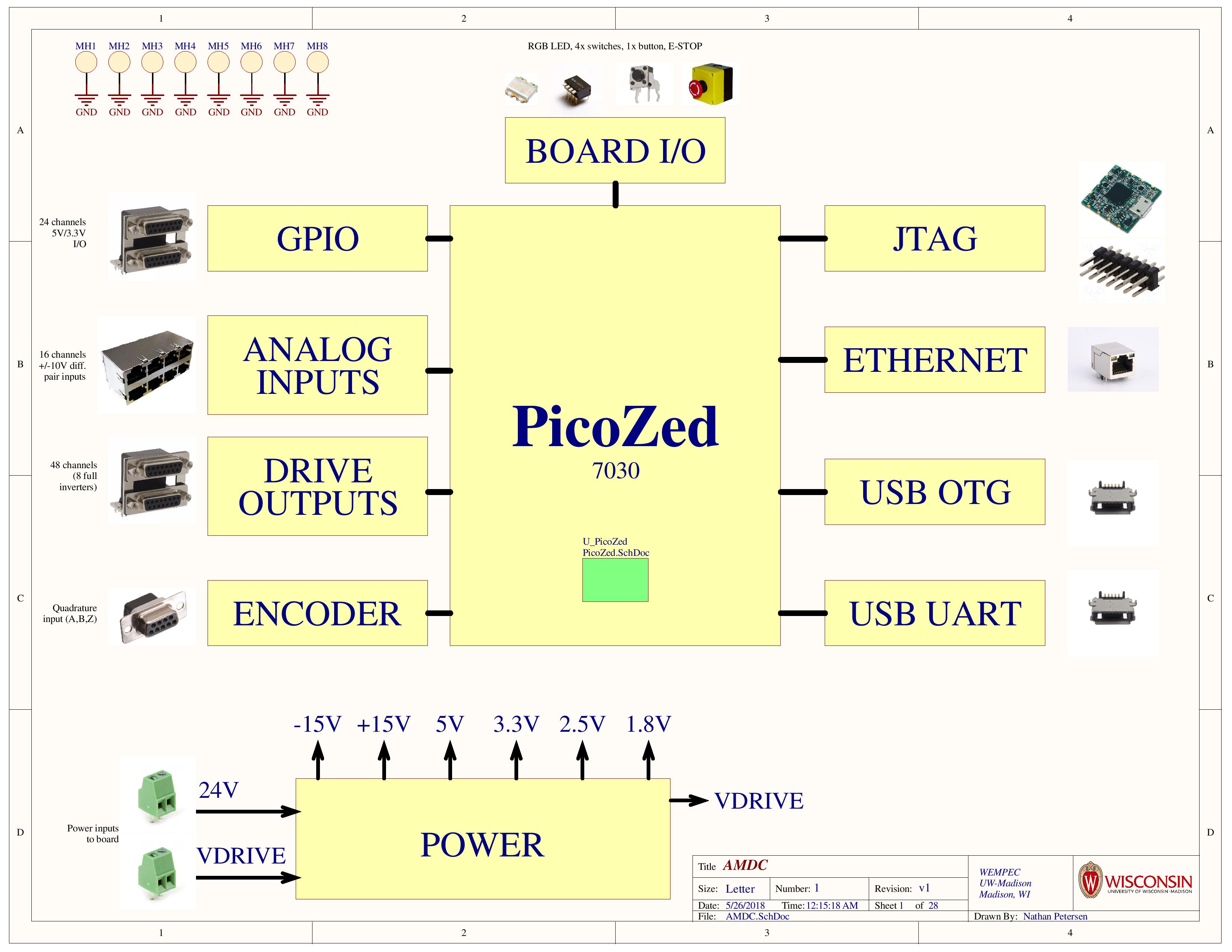
AMDC is a platform which provides relevant interfaces that can be used to control power electronics. Physically, the AMDC hardware is a PCB that serves as a carrier card for a PicoZed SoM.
The provided interfaces include:
- 48 digital output channels (able to provide PWM signals for 8 three phase, two level inverters)
- 32 digital status lines for monitoring the inverters
- 16 analog input channels (+/- 10V differential input)
- 24 general purpose I/O
- Quadrature encoder input
The hardware design for AMDC is completely open-source, with all design files and analysis available on GitHub: Checkout the repository…
I created a PDF report about the project as well: Read the report…
Project Development
Prior to this Independent Study, I had no experience designing analog systems, no experience with Altium Designer, had never done a big board layout, and in general, had never done such a complex project. In order to make this project work, I needed a way to quickly get up-to-speed on the essentials.
Throughout the semester, I worked with Eric and others to create the schematics that would become AMDC. After finalizing the schematic design, I designed the first PCB version for manufacturing. Outlined below are the general steps to the design process that I followed.
Download PDF of entire AMDC schematics…
Circuit Schematic
I used a four-step plan to design the circuit schematic:
1. High-Level Description of Board Functionality
To start the project, Eric provided a set of requirements that the board needed to satisfy. A previous board existed with similar functionality, so he pointed me to the schematics for comparison. The board I was designing was basically an upgrade to the previous board (built upon a newer architecture, more functionality, etc).
2. Generic Schematic Design
At this point, I generically knew the different systems that needed to be included in the design. I started to model everything via schematics in Altium. I didn’t pick precise part numbers for everything and didn’t model footprints or 3-D packages.
The output of this phase was intended to be semi-accurate schematics to discuss and verify correct design direction.
3. Part Search
After drawing up generic schematics, I transitioned to modeling real components that I could purchase and use. I modeled footprints, checked availability, and started doing cost comparisons.
4. Schematic Approval
Now, I had a full schematic that was ready to approve. This was the nitty-gritty part of the design; we needed to make sure every aspect of the schematic checked out before starting PCB layout. I didn’t want to do the layout just to realize the schematic was wrong and have to start over!
In the Schematic Analysis portion of this article, I discuss the final schematic in detail.
Board Layout
For me, designing the schematic was much harder than laying out the board because I actually needed to understand the electrical properties of all the system modules. Once I had the schematic, though, doing the layout wasn’t as challenging; I just needed a reasonable layout that satisfied the Design Rule Check and made sense.
With over 25 pages of schematics and hundreds of components to place and route, I needed a step-by-step plan on how to do the layout:
- Define board size, layer stackup, design rules
- Define board regions for the different modules
- Place connectors/interface components
- Place rest of parts
- Route high speed signals (Ethernet, USB, etc)
- Route delicate analog signals
- Route the rest of signals
- Create power plane for solid power delivery to all regions of board
- Position silkscreen text for labeling jumpers, connectors, etc
- Clean up board, optimize copper pours, etc
All in all, I designed the whole PCB in just 14 days, spending about 6 hours a day on it for a total of around ~60 hours. I don’t recommend doing it in such a short time frame. :(
Schematic Analysis
The AMDC schematics can be a bit daunting to understand at first because of the sheer number of pages and systems. I will explain each module in the following section.
As I drew up the schematics, I kept adding more and more sheets for many different modules. The design was naturally hierarchical in organization, so I utilized that structural ability within Altium.
Because of this, designing everything was very modular and much easier to understand; there were no global signal lines spanning across 28 sheets of schematics to track. I really wish my personal EDA tool, Eagle, supported this hierarchical schematic ordering…
PicoZed SoM
The PicoZed System-on-Module (SoM) is a SoM developed around Xilinx’s Zynq-7000 System-on-Chip (SoC).
The Zynq-7000 SoC family integrates the software programmability of an ARM-based processor with the hardware programmability of an FPGA … on a single device.
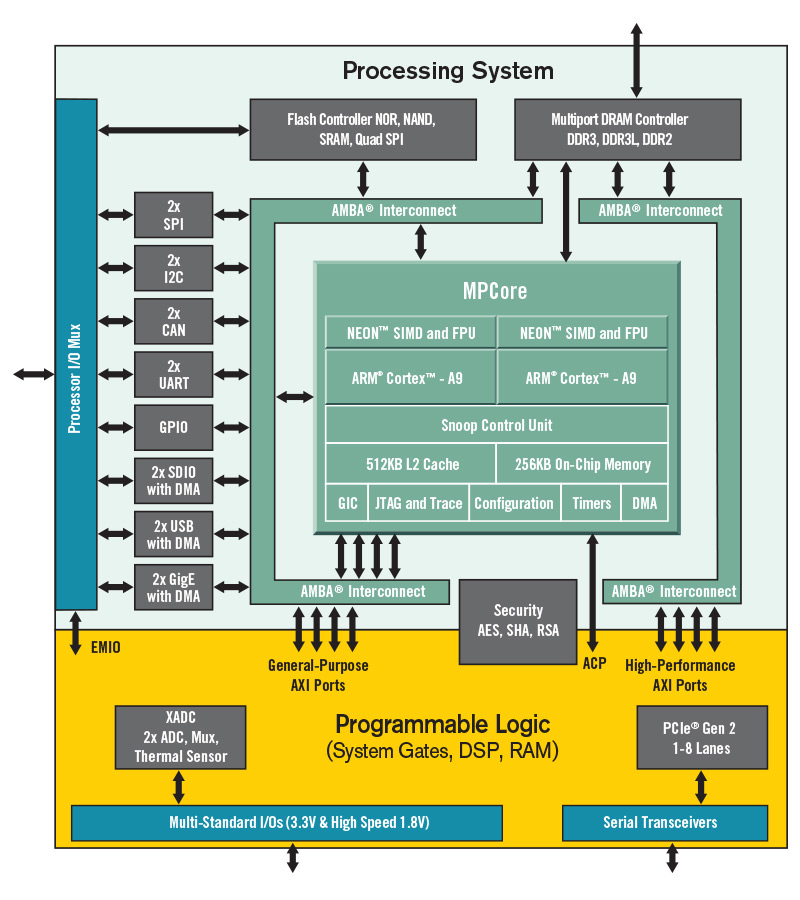
While this SoC is very powerful and capable, it is not easy to integrate into “consumer” projects. It uses a BGA package, which makes soldering difficult, and it requires high-speed routing for memory interfaces. For these and other reasons, the PicoZed exists!
The PicoZed module contains the common functions required to support the core of most SoC designs, including memory, configuration, Ethernet, USB, and clocks. It provides easy access to over 100 user I/O pins through three I/O connectors on the backside of the module.
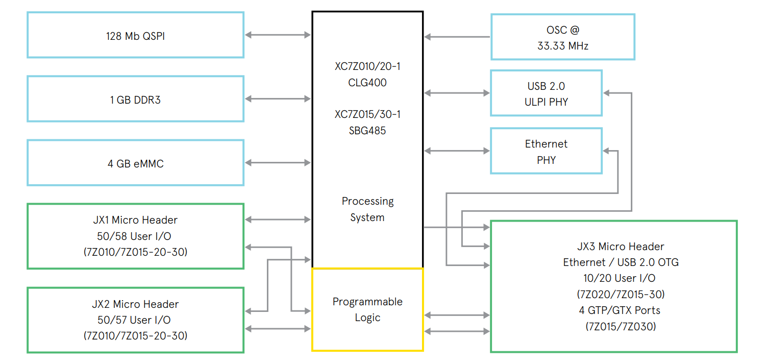
To use the PicoZed, one must design a carrier card to interface with the SoM. PicoZed has great documentation about carrier card design, schematics for reference carrier cards, etc.
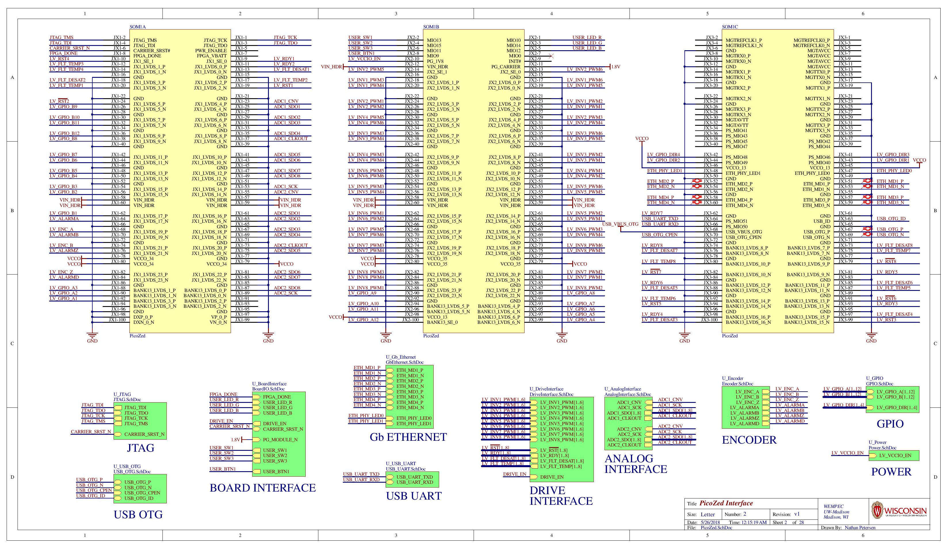
PicoZed Interface
Since this is a carrier card, there are many signals needing to flow in to and out of the PicoZed SoM. This makes for a lot of signal connections (~300!):
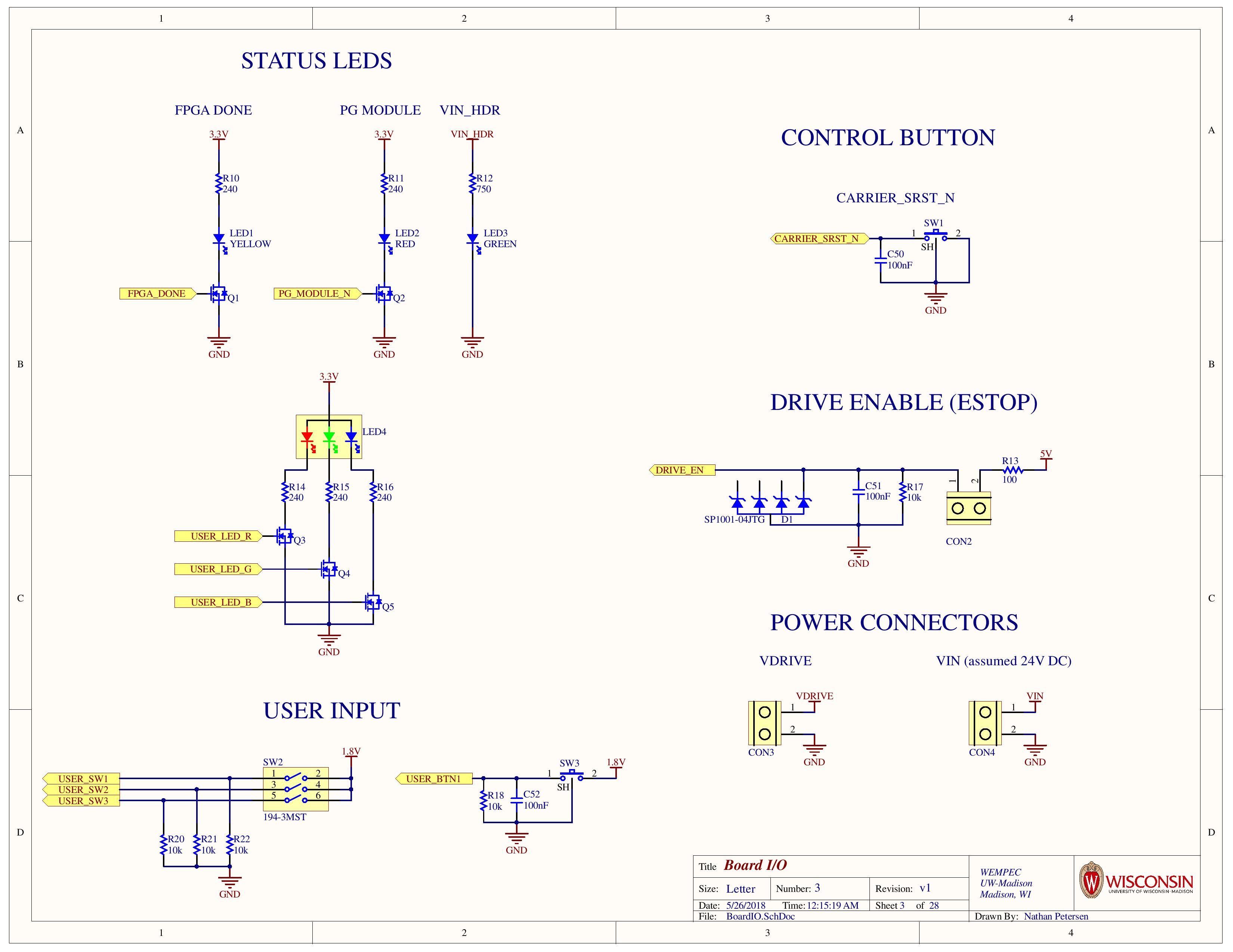
Board I/O
Almost every processing system needs a few things to function:
- Standard reset button for Xilinx Zync-7030 SoC
- Status LEDs to indicate board state
- RGB LED controllable via processor
- 3 DIP switches
- 1 general push button
- ESTOP button for disabling drive output
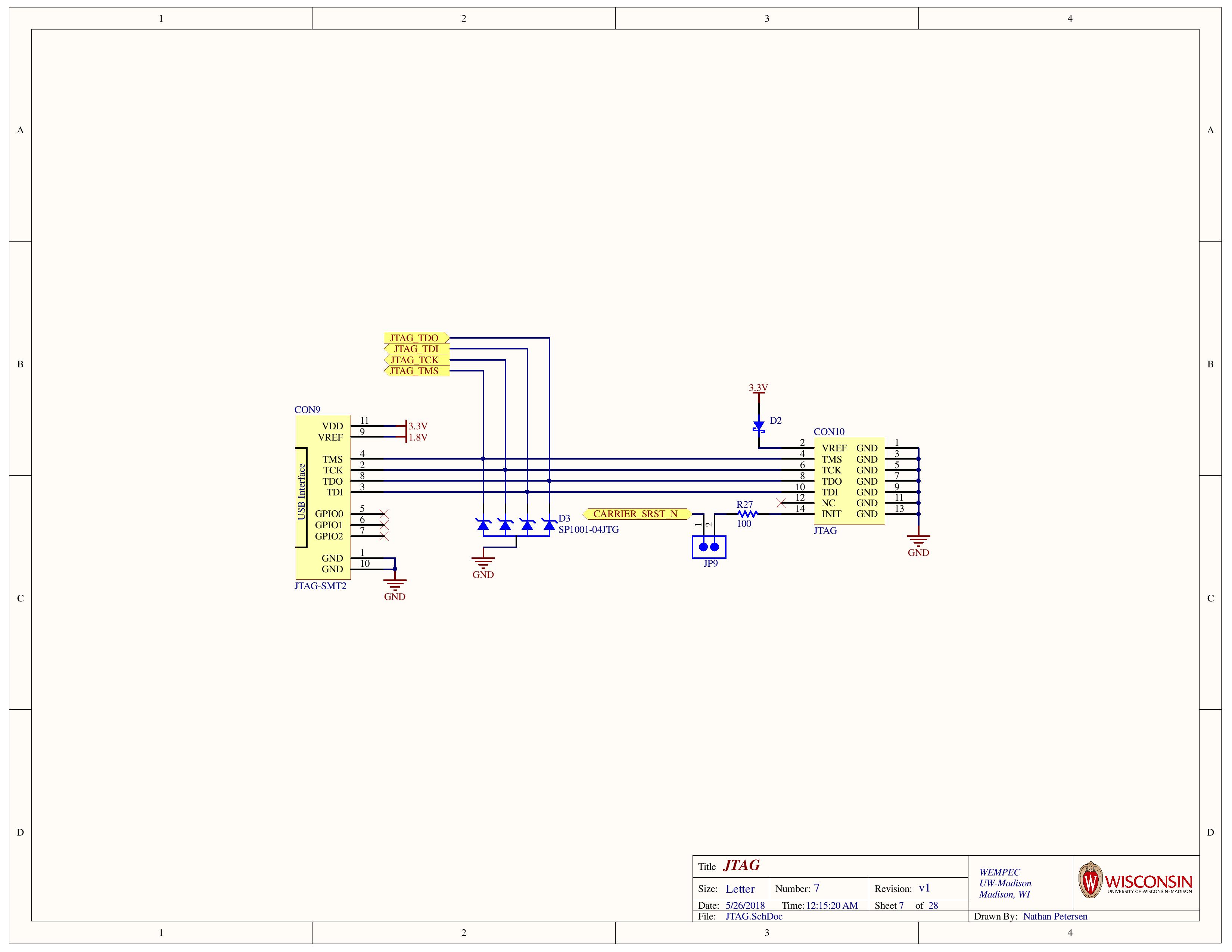
JTAG
To support easy programming and debugging, a Digilent JTAG-SMT2 module is used. This converts micro USB into JTAG signals for the processor. The board also includes standard 2x7 headers for using an external JTAG programmer.
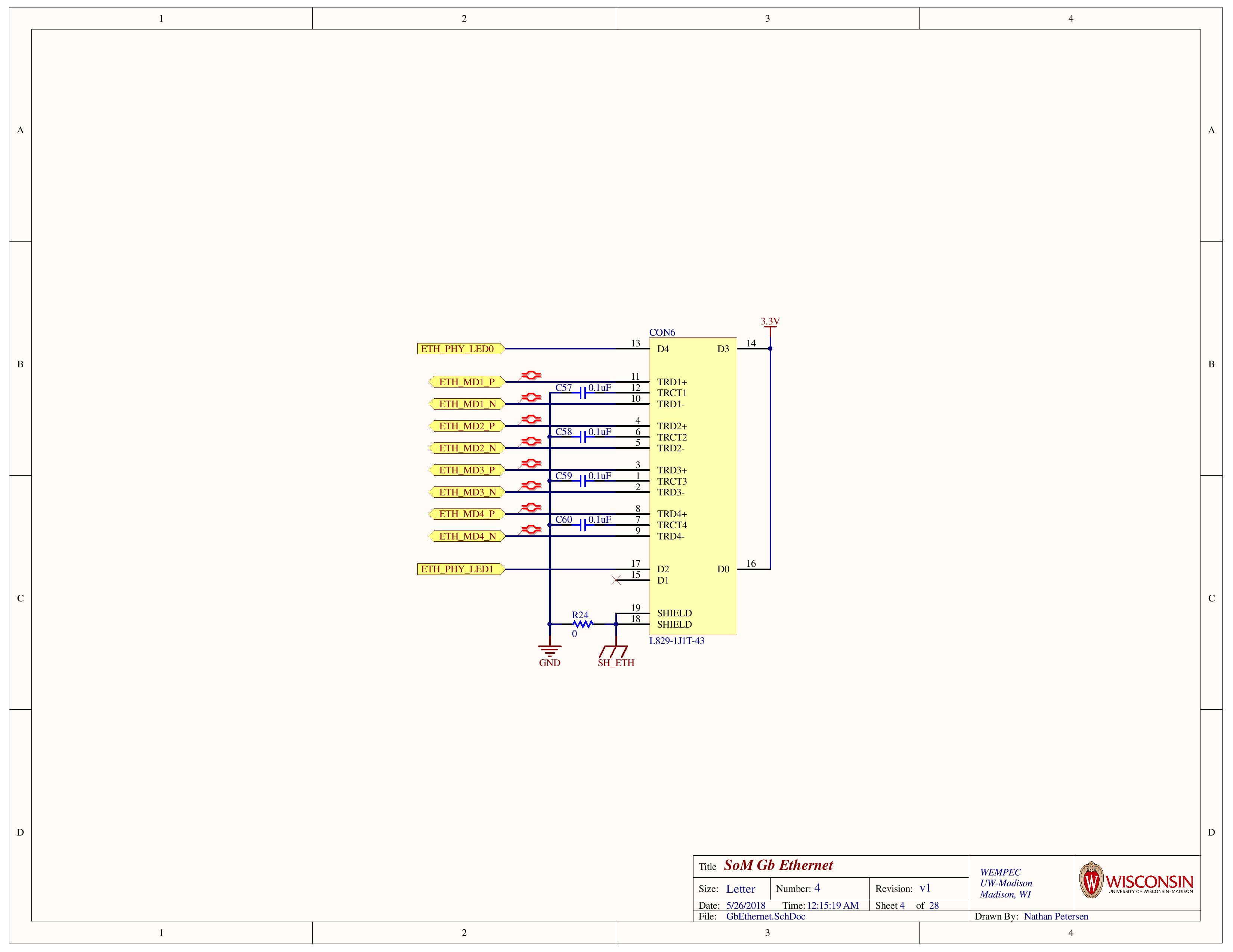
Ethernet
PicoZed has an Ethernet PHY onboard the SoM, so it exposes data signals that go directly to a connector. All that’s required on the carrier card is routing them to a RJ45 receptacle.
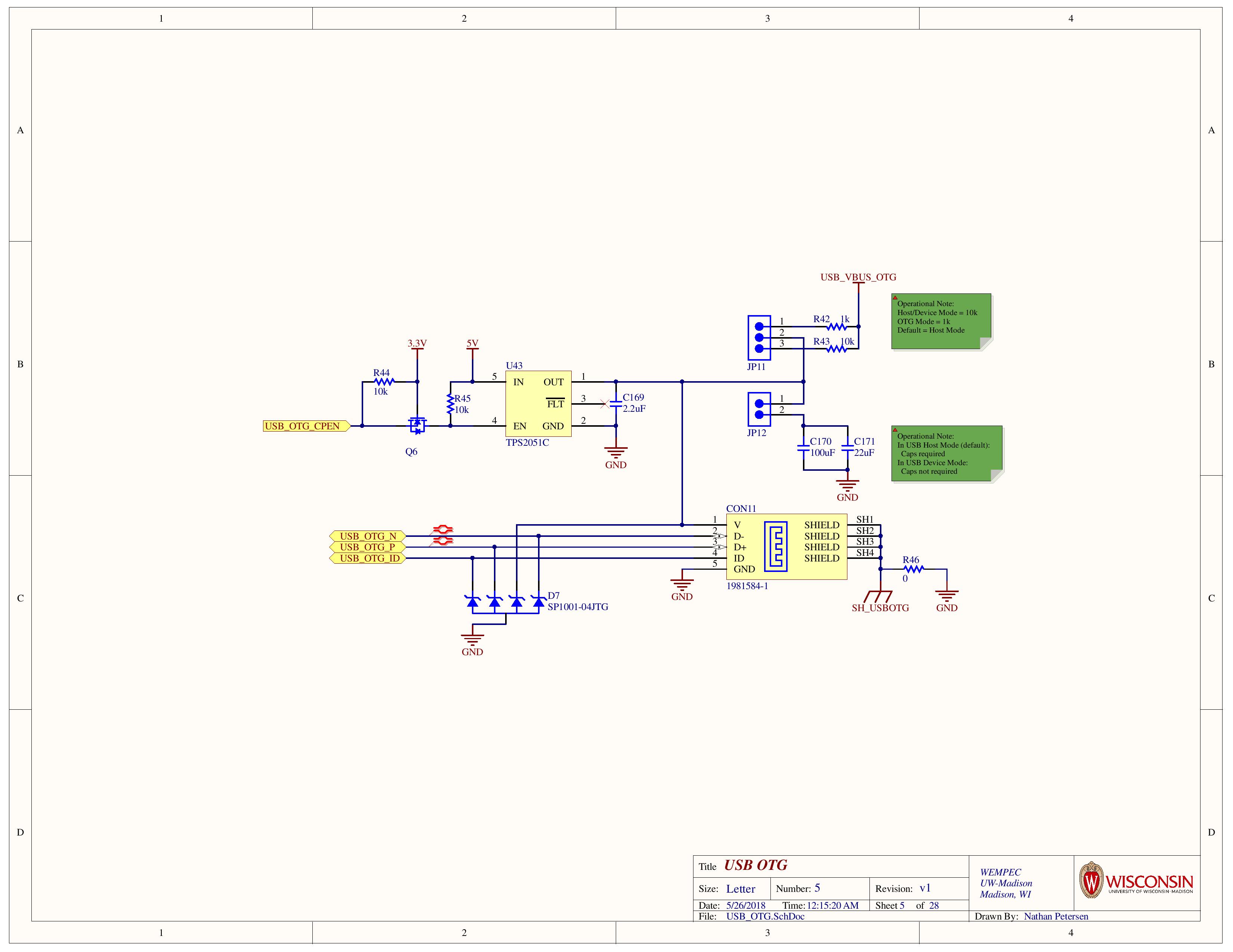
USB OTG
PicoZed also has a USB On-The-Go (OTG) PHY on the SoM, so again, the carrier card just needs to route out signals to a connector.
AMDC includes extra circuitry for USB protection. This prevents external devices from drawing too much current, adds ESD protection, and adds the ability to select between Device / Host modes.
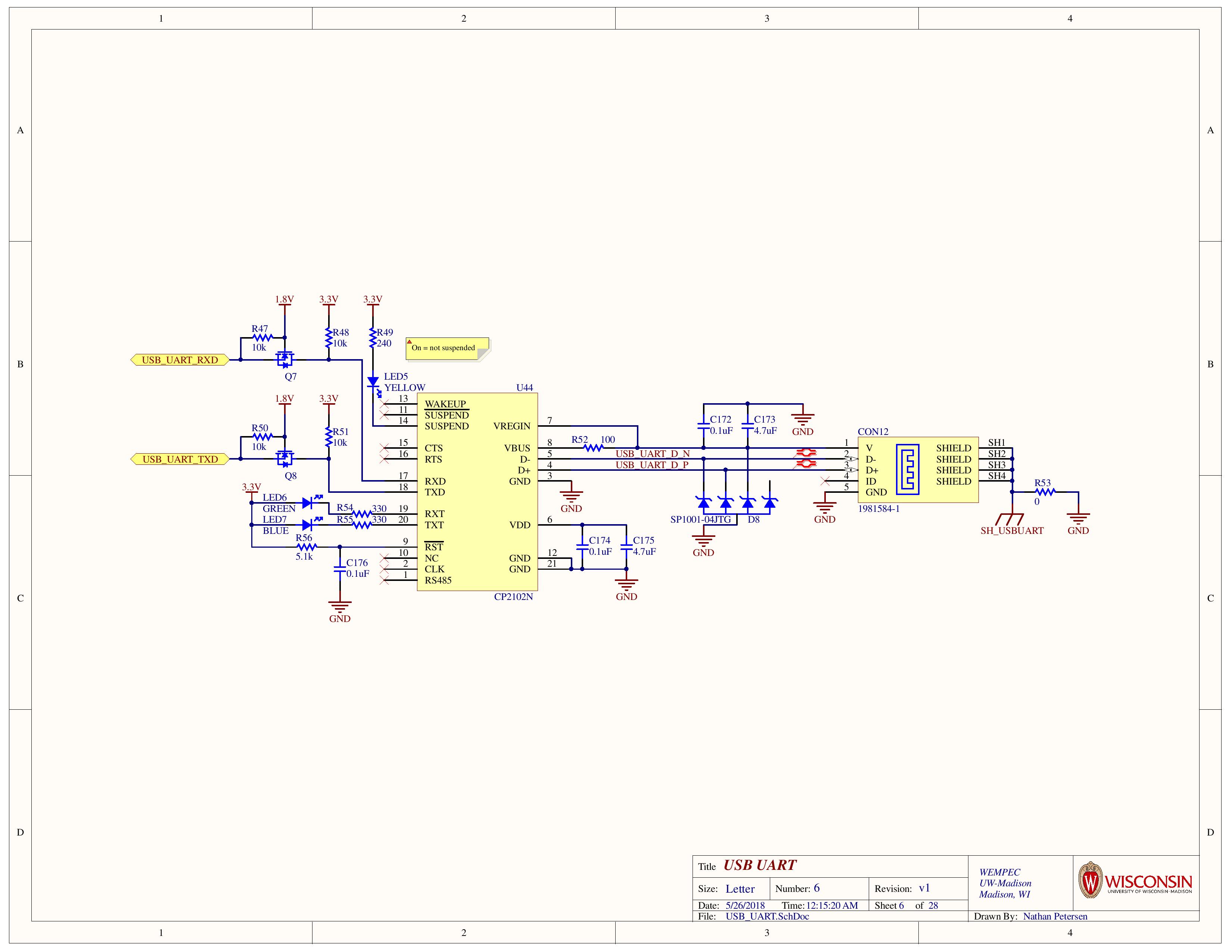
USB UART
For serial communication with the ARM core onboard (i.e. communicating with terminal running on embedded Linux OS), a micro USB port is provided which interfaces directly with a UART port. This uses a Silicon Labs UART to USB device for simplicity.
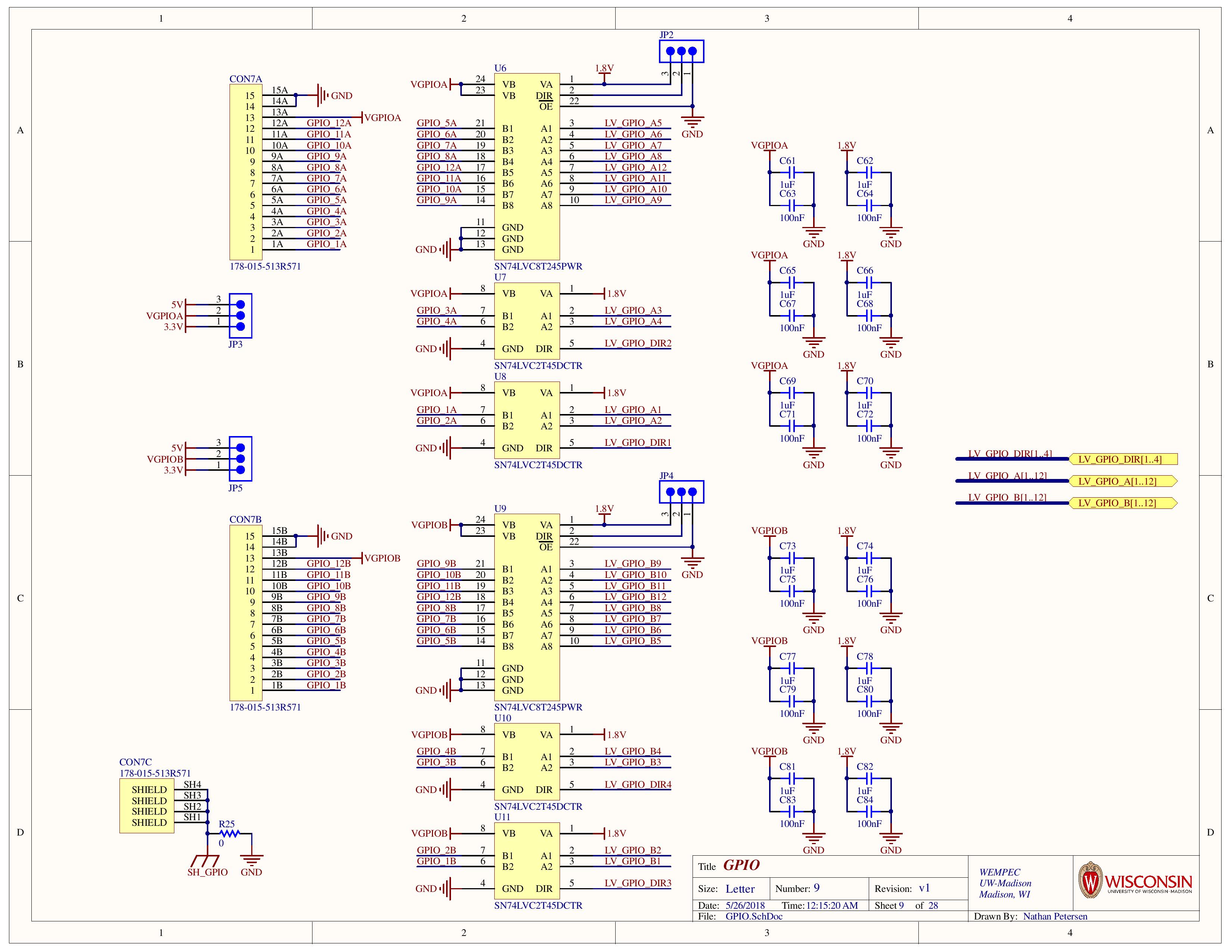
GPIO
While the main bulk of AMDC’s design is for its drive outputs and analog inputs, not all applications strictly use these interfaces; some need general purpose I/Os for various other modules.
AMDC provides two banks of GPIO, with each settable at either 5V or 3.3V logic levels.
Each bank has 12 channels:
- 8 channels have a hardware pin selectable direction
- 2 x 2 channels have a software selectable direction
Analog Inputs
AMDC has unique constraints for analog signal inputs (+/- 10V fully differential). To support this wide range of voltage, analog conditioning circuitry must be used.
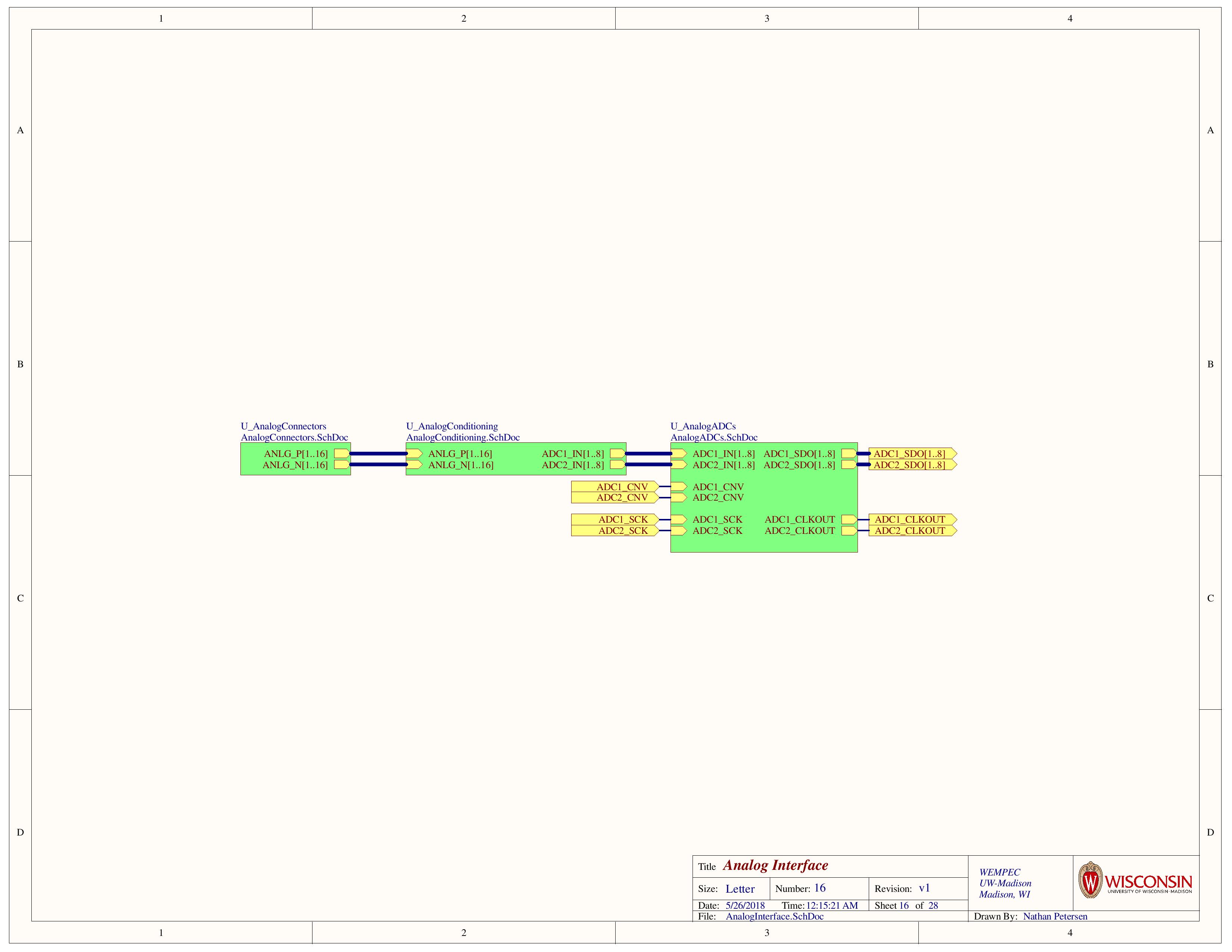
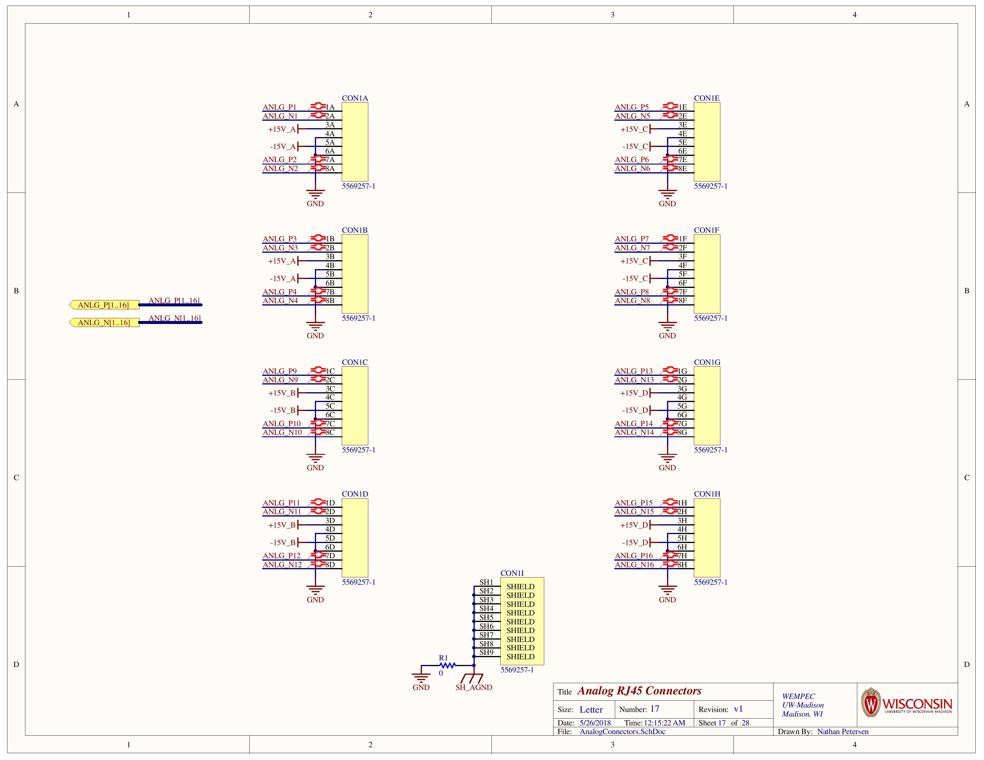
Analog Connectors
Starting at the analog input connectors, there are 16 channels which appear as a stacked 2x4 RJ45 receptacle box.
Analog Signal Conditioning
The analog signal inputs from the connectors then go through a signal conditioning block which converts the +/- 10V fully differential signals into 0V..5V pseudo-differential signals for the ADC to process.
Two different signal conditioning blocks are used to evaluate different conditioning topologies.
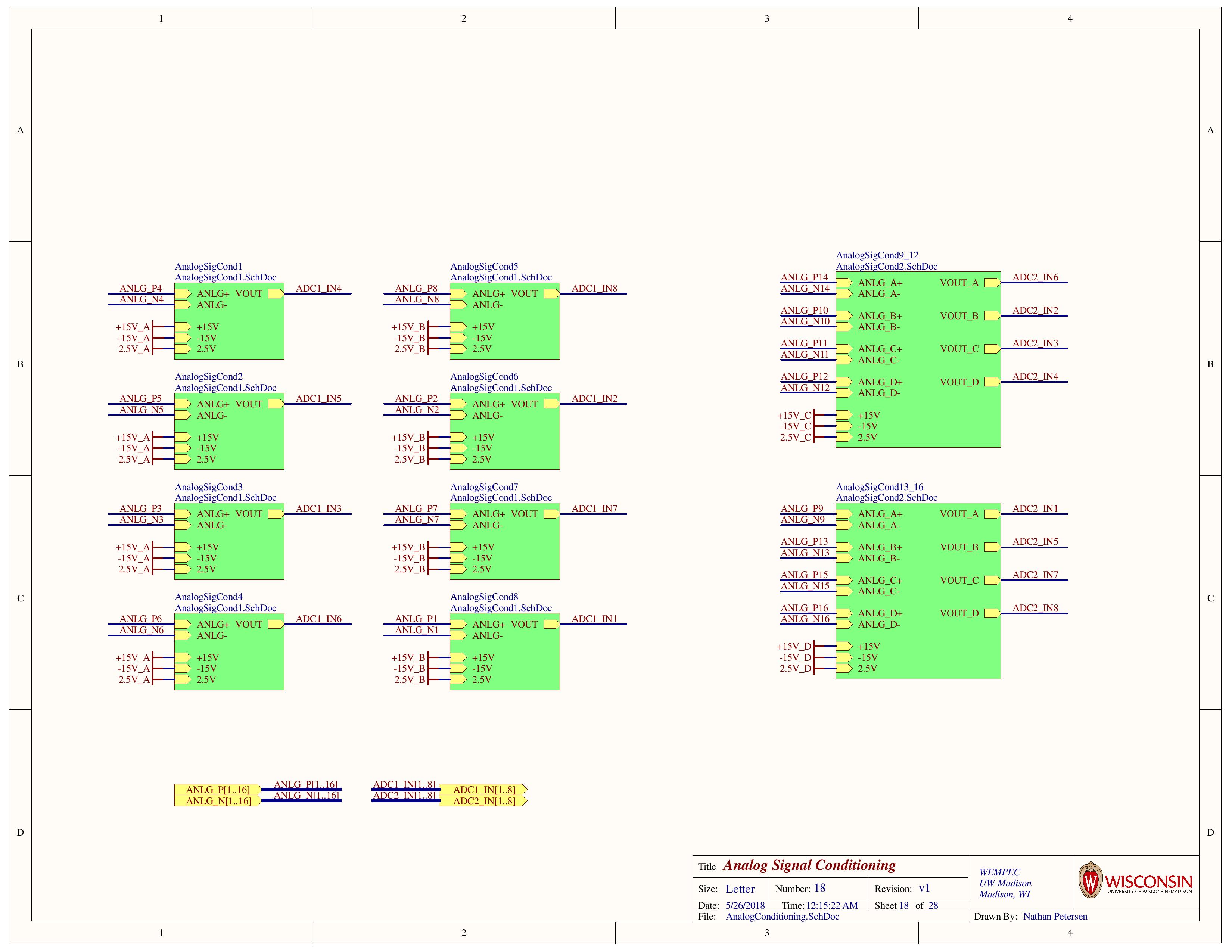
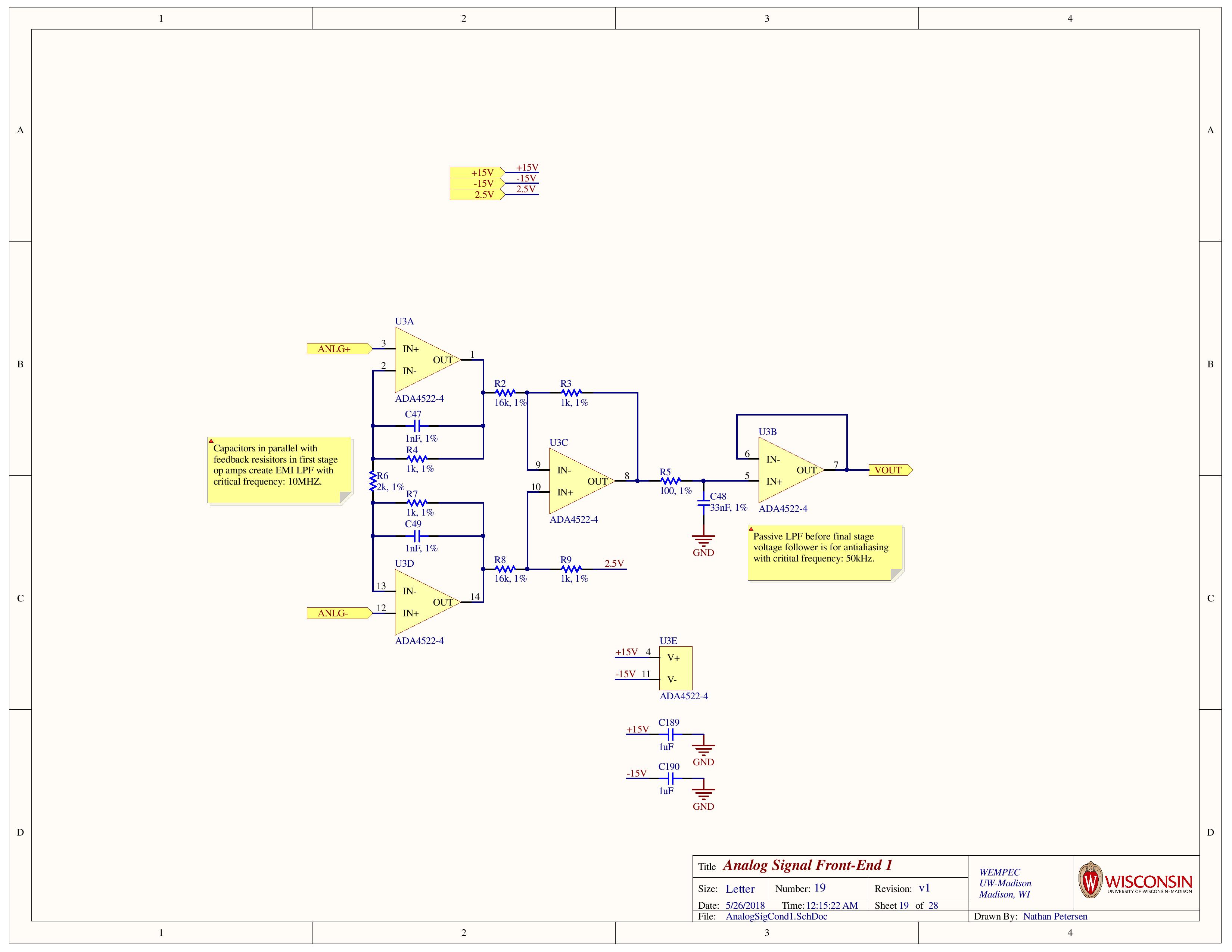
Signal Conditioning Approach #1:
This approach is used for channels 1 to 8. It uses discrete quad op-amp packages used to create an in-amp topology. Because of the custom in-amp construction, AMDC can exactly condition +/- 10V signals into the 0V..5V range required by the ADCs.
Unfortunately, the performance of this topology depends on the tolerance of the resistors used. We must precisely match resistor values otherwise there is poor common-mode voltage rejection.
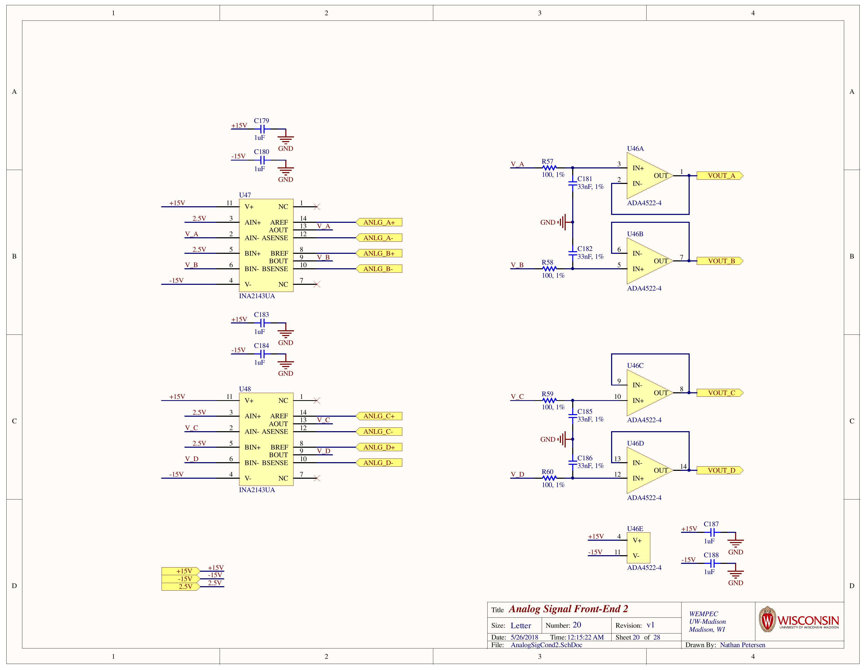
Signal Conditioning Approach #2:
This approach is used for channels 9 to 16. It uses integrated in-amp devices which have laser-trimmed resistors. Because of this, there is very high common mode voltage rejection, but at a fixed 0.1x gain, this is not ideal for +/- 10V signals.
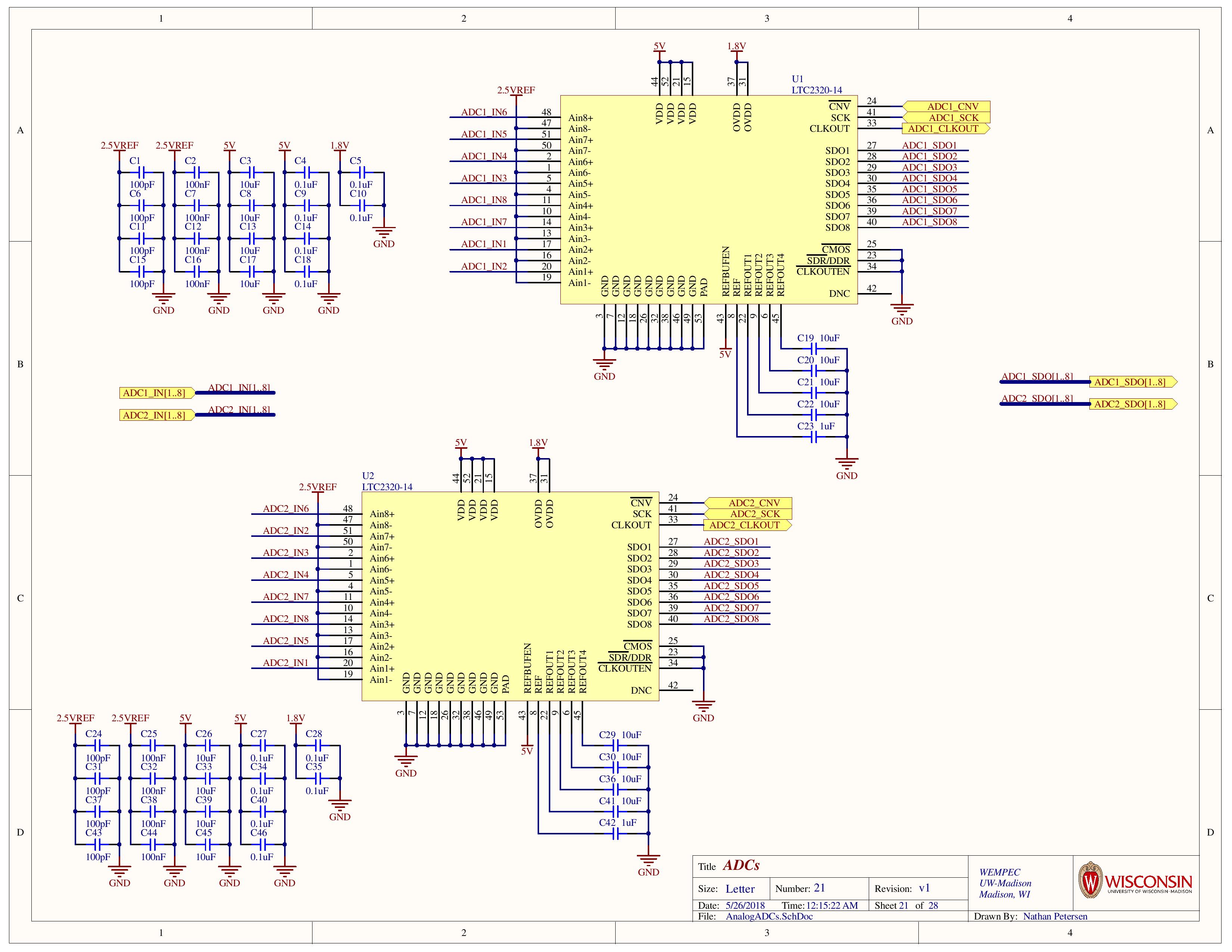
Analog ADCs
After signal conditioning, two 1.5 MSPS 8-channel ADCs are used. These provide a partially parallel digital interface to the PicoZed for sample data.
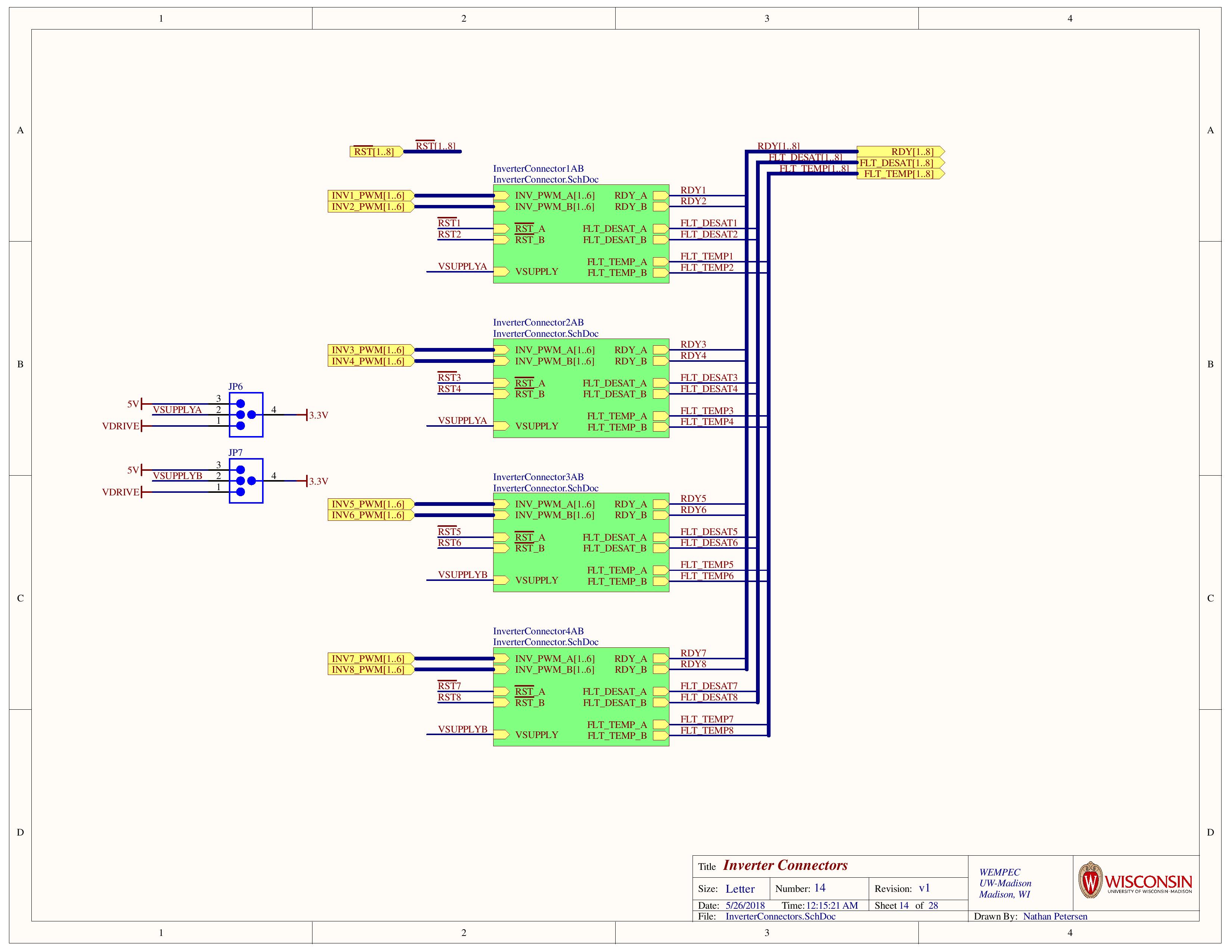
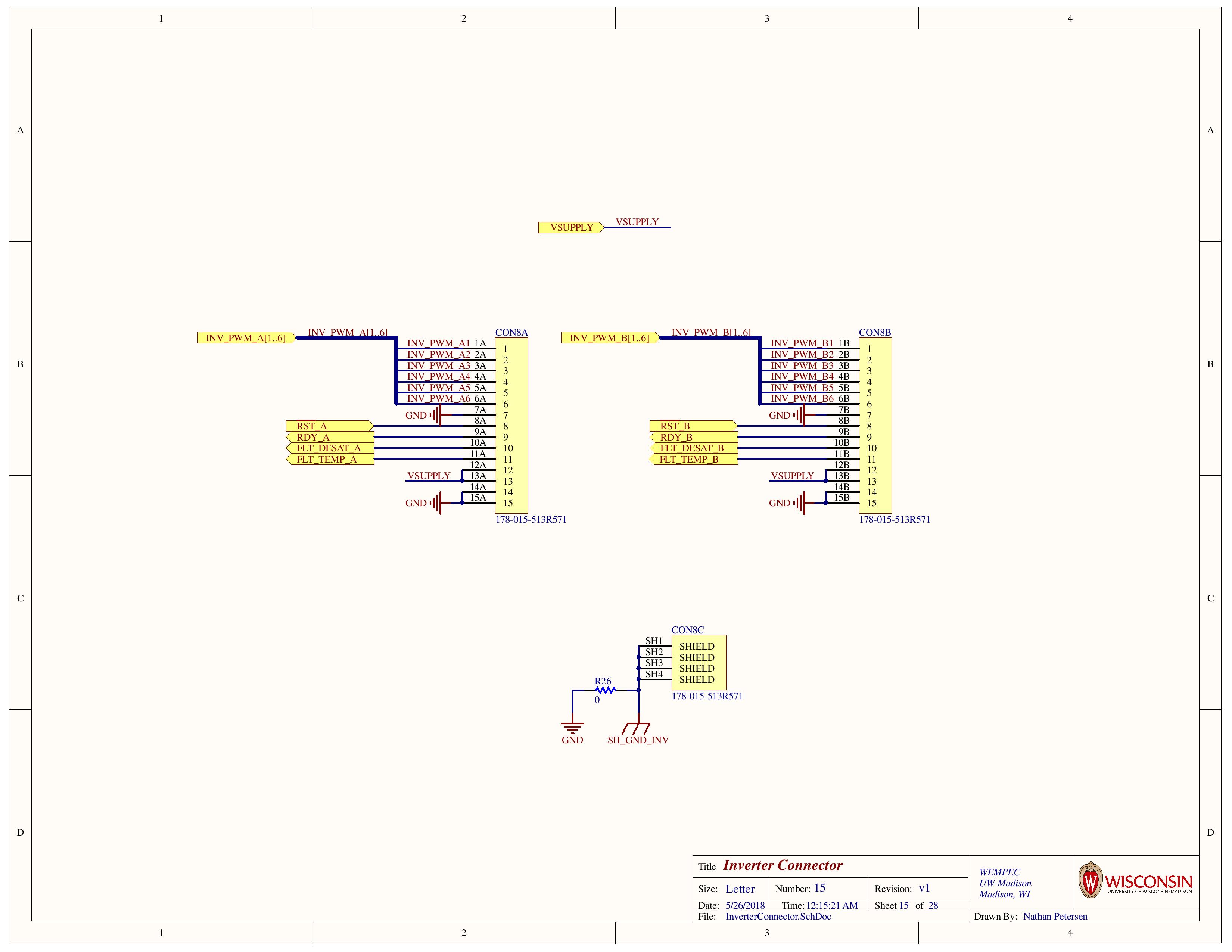
Drive Outputs
AMDC can control eight full inverters at one time via eight DB15 connectors. The design targets controlling Wolfspeed modules (each 15 pin connector controls one module). There are six PWM gate signals, and four status lines.
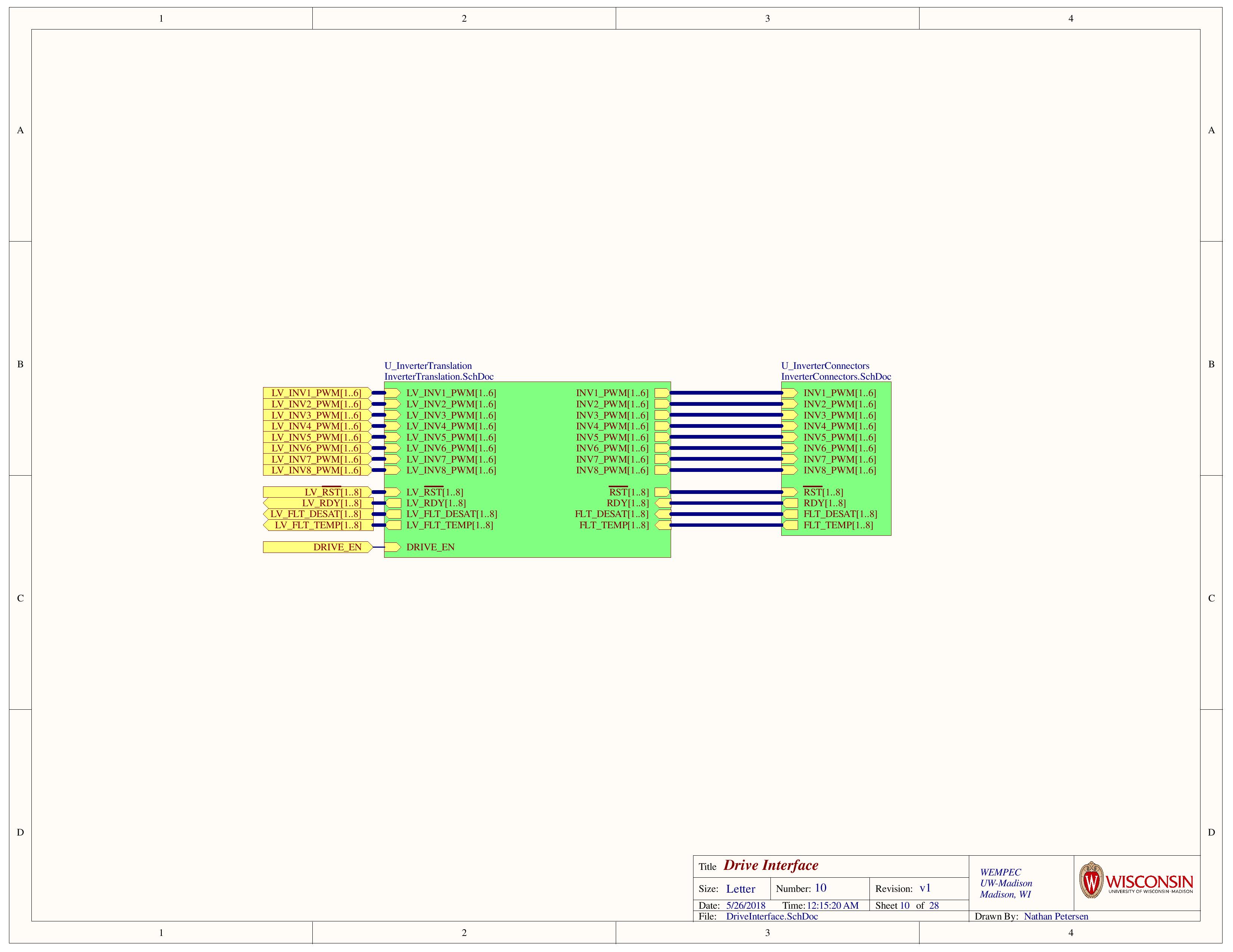
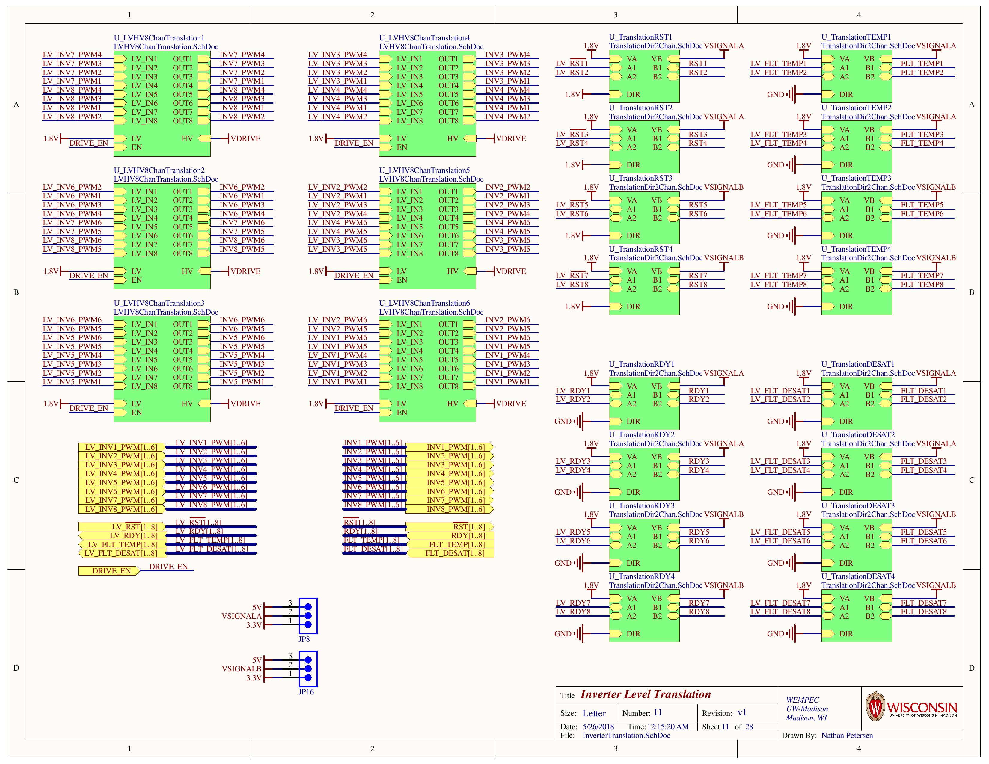
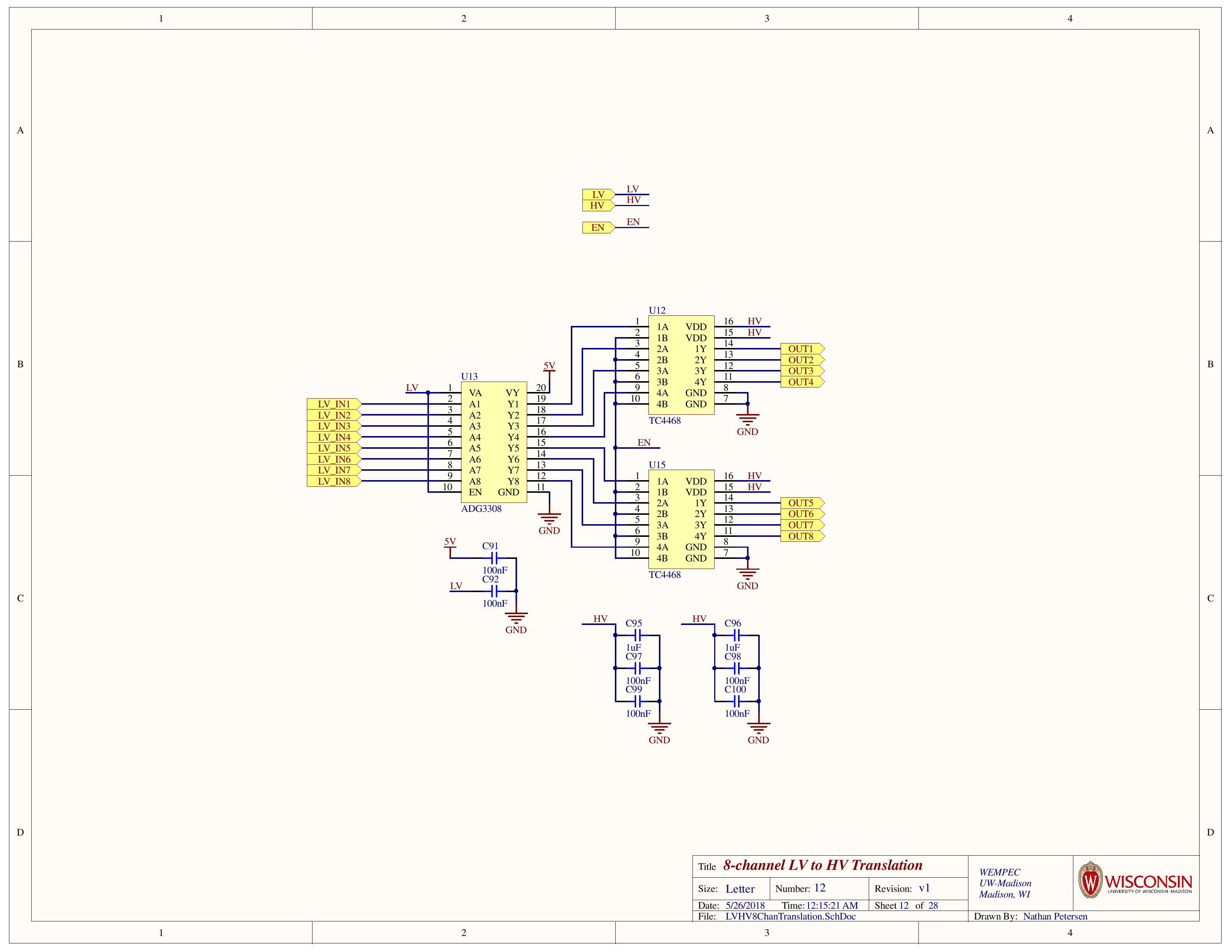
Drive Voltage Translation
For the PWM gate signals, PicoZed outputs digital signals at 1.8V. Voltage translation blocks then boost this signal up to a user supplied output voltage to go off the board (~15V).
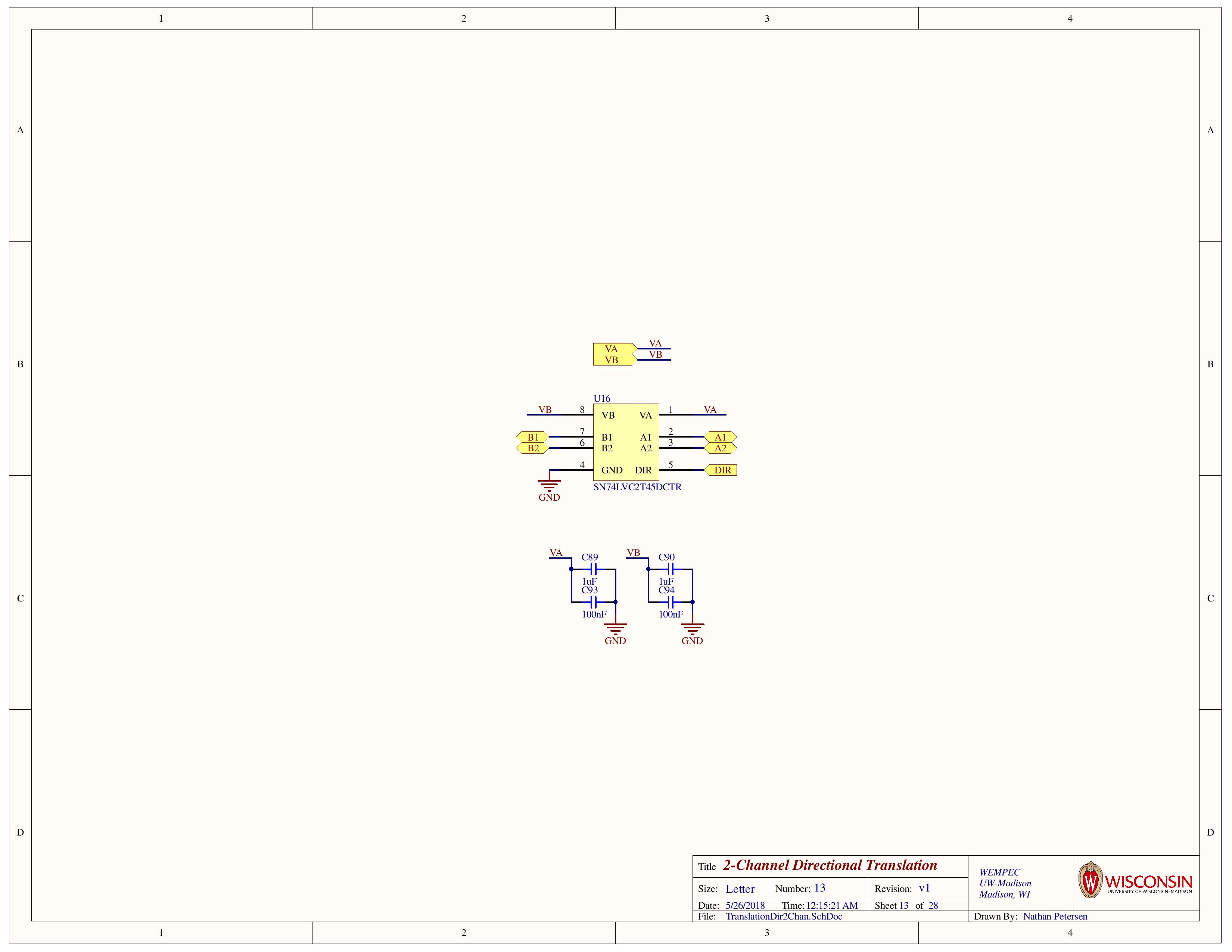
There are hardware selectable status voltages to/from inverter modules to allow interfacing with a broader range of modules.
Drive Output Connectors
Each inverter uses one DB15 connector. To save board space, these are stacked to form four stacks of two DB15 connections each.
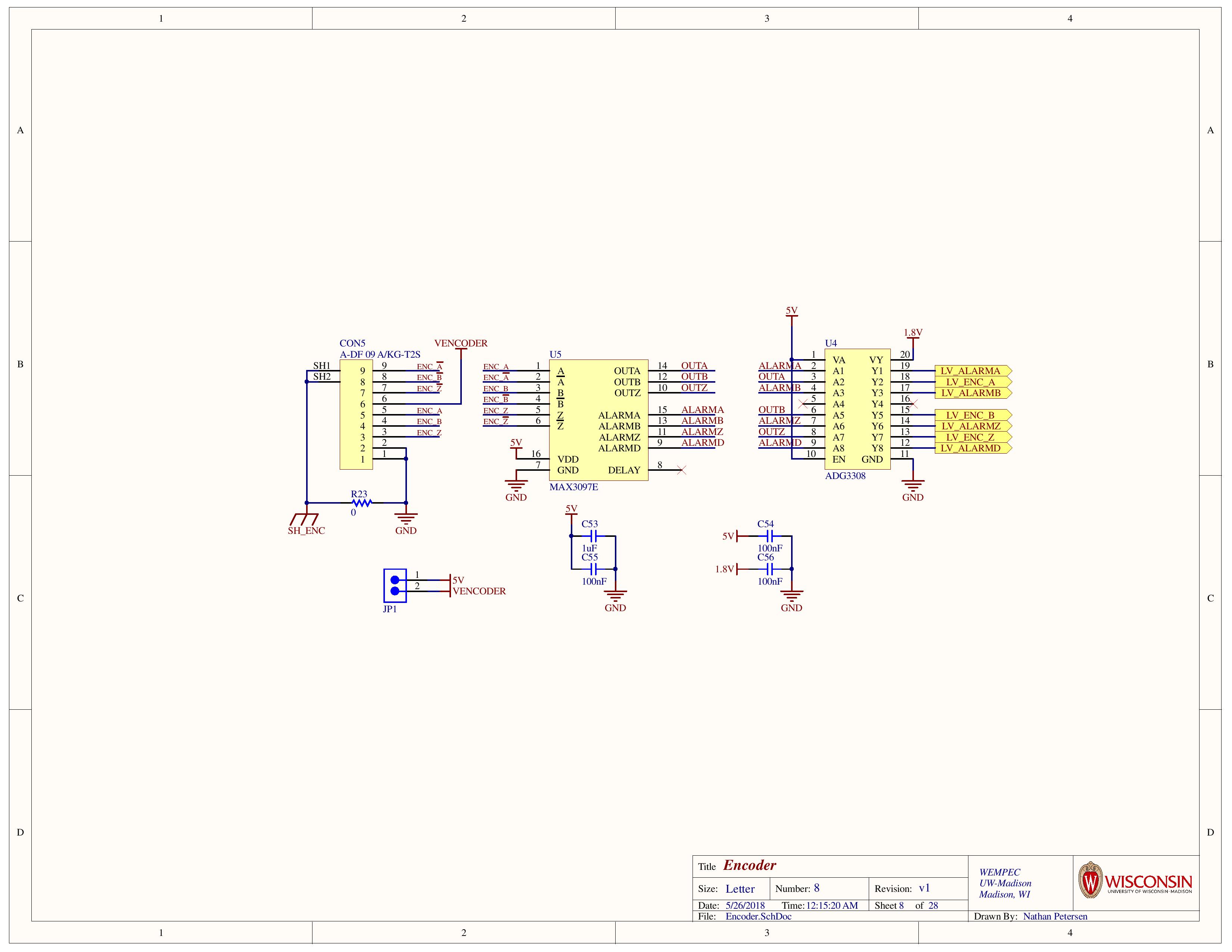
Encoder
AMDC supports connecting one RS-422 standard quadrature encoder through a DB9 connector.
Power
AMDC has two main power inputs: the main board power (~24V) and the PWM drive output voltage (~15V).
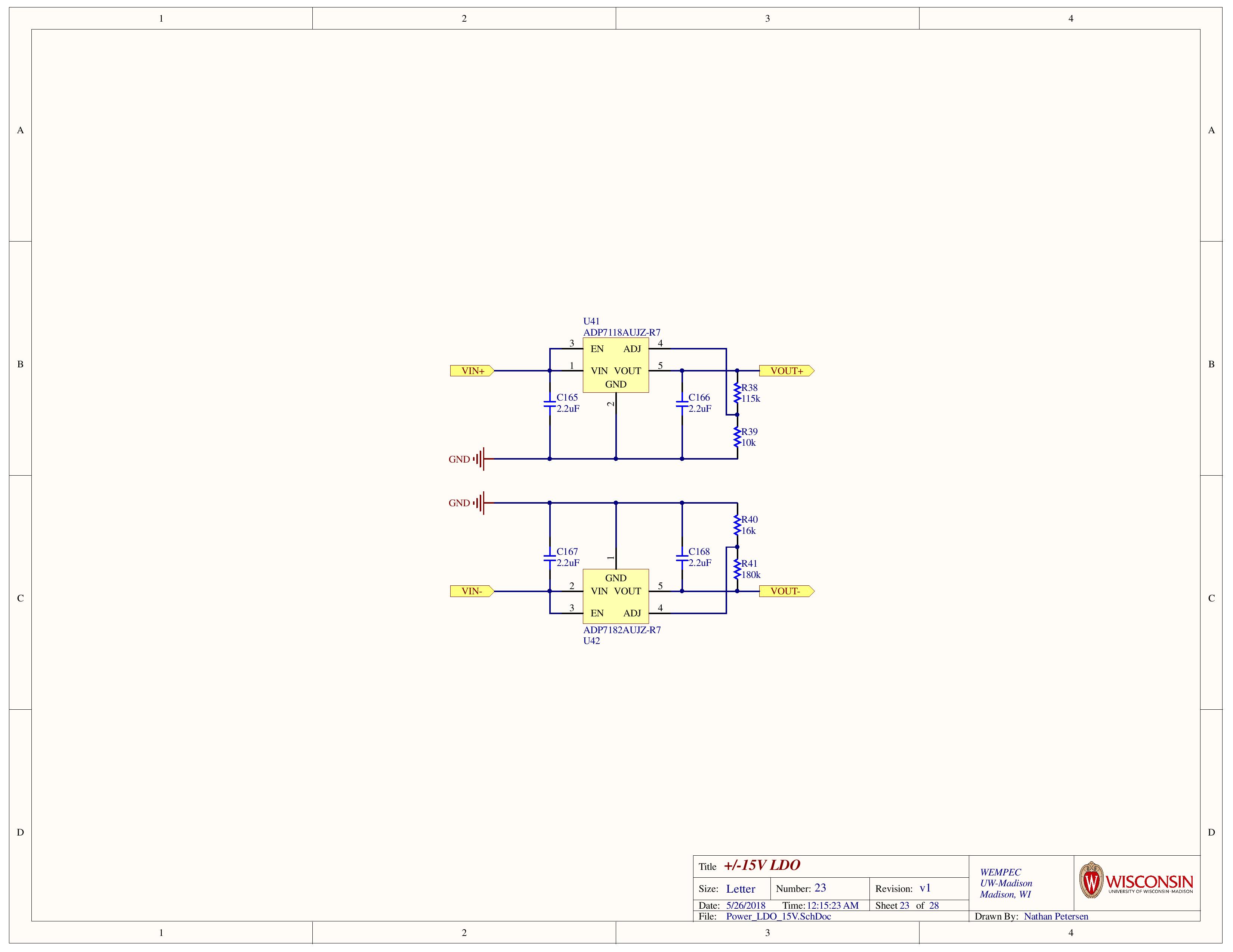
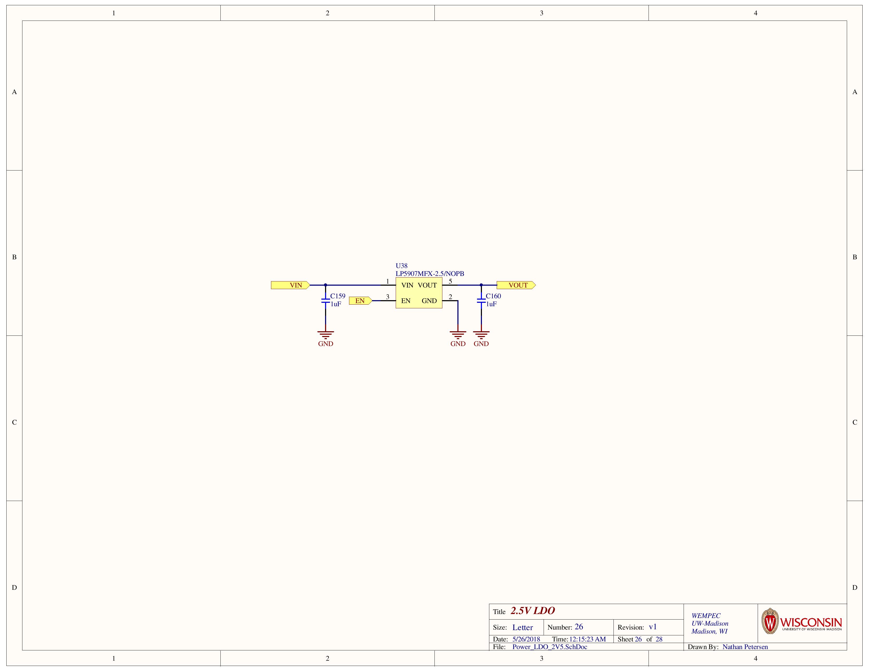
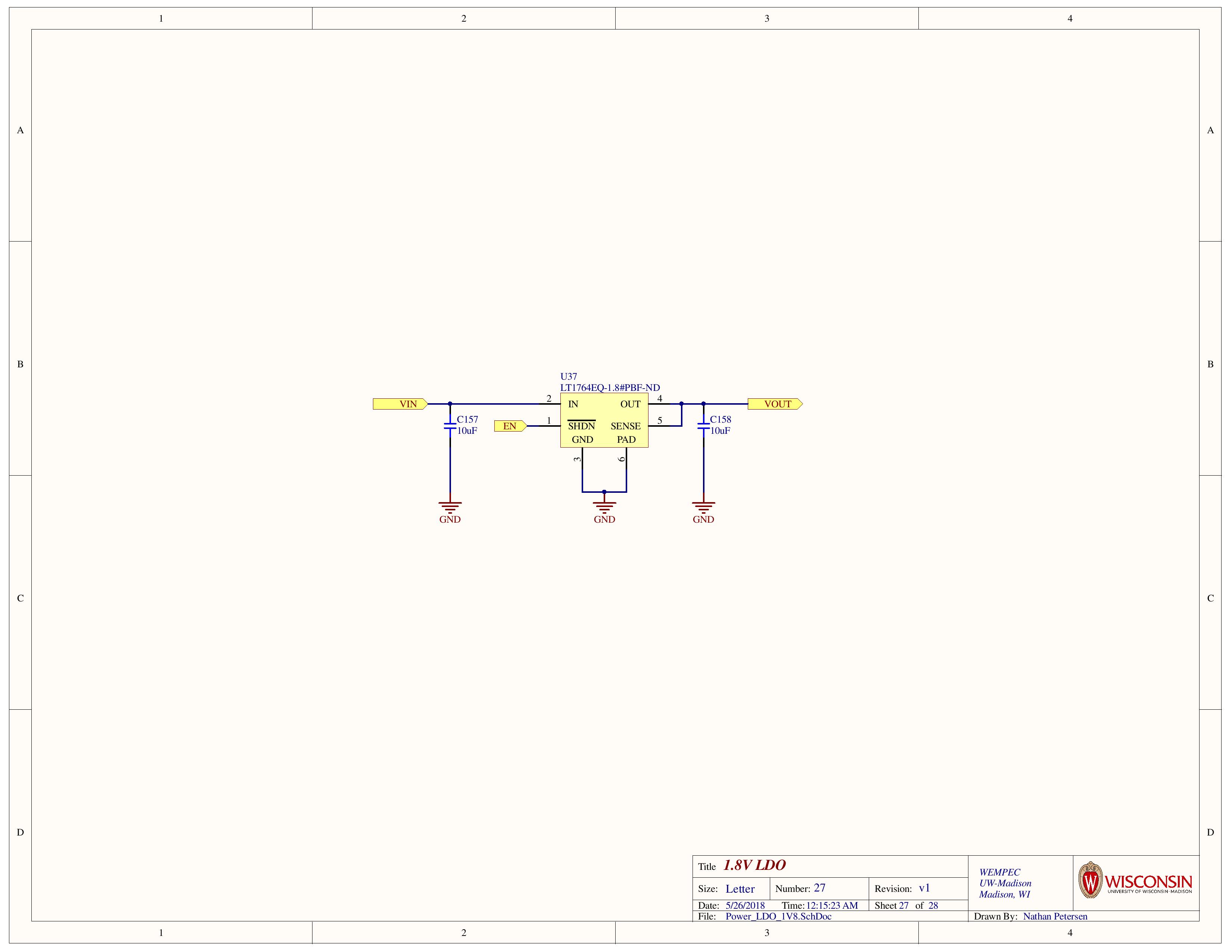
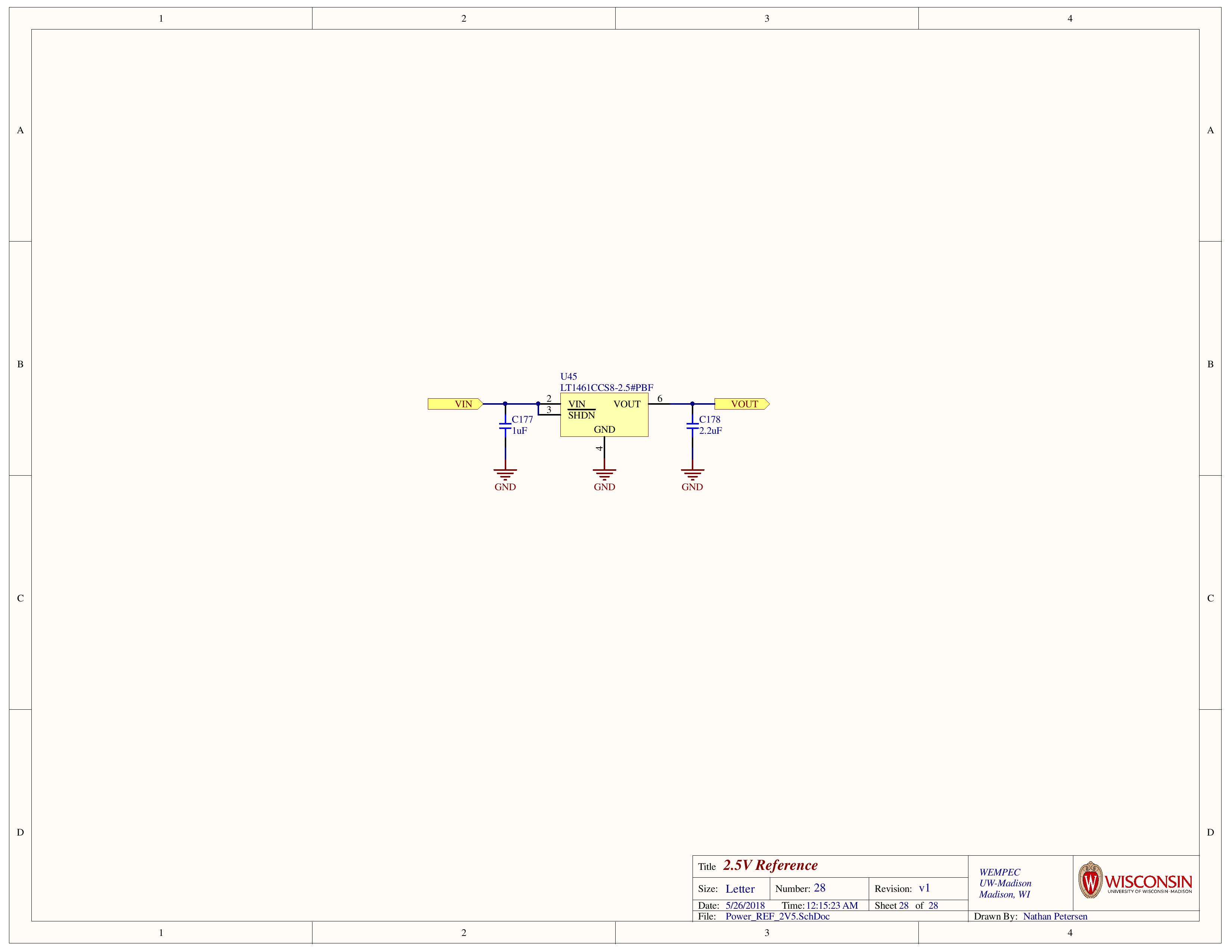
The main board power goes into two DC/DC converter modules which efficiently convert the 24V to 5.5V main power and +/- 16V for the analog systems. These secondary stage voltages are considered “dirty” due to the switching converter design, so many local LDOs provide “clean” device power throughout the board (5V, 3.3V, 1.8V, 2.5V, +15V, and -15V).
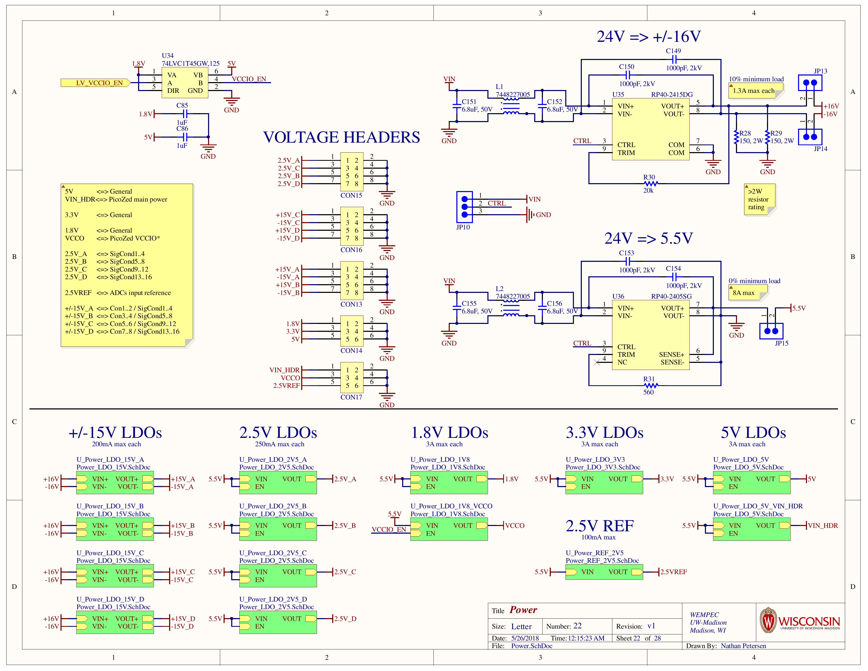
LDOs
Because of the large number of subsystems, six different LDOs are used to target various voltage levels.


PCB Analysis
The AMDC system is designed to be used in a research setting, mounted in a server rack along with other power electronic PCBs. This constraint defined the size of the board, as well as the interface connector locations. The PCB fits in a 1U server rack, meaning it measures about 5” by 17”. All the connectors are accessible at the front of the board.
For Design Rules, I targeted widely available processes that basically all fab houses can do: 6/6 mil clearances, 0.3mm minimum drill, and four layers with 1oz copper. This means the board can be manufactured for cheap by many PCB fabricators. We ended up ordering the board from an American company because of higher reliability and shorter turnaround times.
To protect the integrity of the analog system, all analog parts and traces were placed on one half of the board.
Fun Altium Features
I played around with length matching traces for high speed signals in Altium. After reading tutorials online, it was very easy to set up and use! I length matched the Ethernet differential pairs coming from the PicoZed connector to the RJ45 receptacle.
After some research, I learned that putting bends in traces to do length matching is actually not always a good idea. If the traces carry high-speed content, the corners of these bends emit RF spurs related to the frequency of the content. In a low-noise environment, this can be very bad. The power electronics research environment for which this board is targeted is inherently noisy, so the added PCB emissions have minimal effect.
Summary
Wow. This was a huge undertaking for me as an inexperienced undergrad. I remember multiple times at design meetings when Eric and others would ask me questions, thinking that I was the expert on the design and would know the answers. It took me a while to realize that, yes, I was the design expert and it felt good to be able to answer their questions about things that, just weeks before, I knew nothing about.
I’m very happy with all the skills I’ve acquired throughout the process and greatly indebted to Eric for letting me learn via his project.
You may be wondering if this design actually worked… Well, I ended up designing the PCB after the Spring semester ended and then left for my summer internship before the board was fully assembled and tested. Another grad student took over the project for the summer and ended up creating revision 2. I had used some incorrect footprints that didn’t fit the desired parts, as well as using too powerful of DC/DC converters, thus adding unnecessary cost to the BOM. He addressed these problems and started work on the next iteration of the design. All that said, my original design was never fully tested; it was assembled, and the aforementioned physical bugs were found and addressed.
I look forward to returning to Eric’s research group this fall to work on the embedded firmware to run AMDC. Stay tuned for more articles about my adventures!
New Post Notifications
If you read this far into this article, you might be interested in subscribing for email notifications about future new posts I write. I will never spam you! Every few months, I write a new article for this website, and will send you email about it. You can unsubscribe at any time. Thank you.