

Interning at Silicon Labs, the Sequel - Summer 2018
Silicon Labs has sold their I&A Business.
My entire expereince at Silicon Labs, as discussed below, was in the I&A division. Therefore, everything I say below is outdated, since the business/products no longer exist from Silicon Labs.
Most links in this article to silabs.com are now invalid, but I will keep them intact for posterity.
NOTE: Make sure you read this post after reading about my previous internship experience at Silicon Labs.
…And that wraps up my second summer at Silicon Labs! I was there one year ago, during the Summer of 2017, and decided to return for another internship experience.
Having already spent a summer interning at Silicon Labs, this summer felt like coming back to a welcoming home; I already knew most of the people, I already knew the work environment, I was already familiar with the projects being developed, etc…
Once again, I learned a lot about many things:
- New digital radio standards and implementation
- Professional PCB design and project flow
- Internal “productization” of tools for team usage
- Various business units within Silicon Labs
- Other intern projects and activities
- Chain of command within team structure
Read on to learn more about these exciting topics!
WARNING: These are my thoughts and opinions! I do not speak for Silicon Labs as a company. Take what I say with a grain of salt and a pinch of pepper.
About Silicon Labs
Before diving into my summer projects and experiences, I should give a vague notion of what the company, Silicon Labs (www.silabs.com), actually does… According to the marketing people at Silicon Labs:
Silicon Labs is the leading provider of silicon, software and solutions for a smarter, more connected world.
or
Silicon Labs is a family of hardware and software engineers and innovators dedicated to solving customers’ toughest embedded design challenges with breakthrough energy-friendly, connected solutions.
Basically, this means that they are both a semiconductor company (i.e. they design integrated circuits), and a software company (i.e. they write code for these ICs). Silicon Labs makes a wide variety of products targeted at various markets ranging from IoT end-node devices to datacenter timing solutions.
Personal Interest
One of their popular products, the EFM32 series of microcontrollers (MCUs), is of special interest to me. I am actively designing new personal projects incorporating Silicon Labs’ MCUs as the main brains.
After researching their product line and comparing it to the MCU family I currently use, I discovered that Silicon Labs’ devices:
- Cost less for low volume
- Consume less power
- Have better documentation and examples directly from the OEM
Also, not many hobbyists are actively using Silicon Labs’ devices, meaning that my projects could provide example implementations for other people to follow. Because of all these reasons, Silicon Labs got the design win for my future projects. Plus, it’s nice to support them; I spent two summers there after all!
More on Silicon Labs
If you’re interested in learning more about Silicon Labs, I suggest giving their 2018 Q3 corporate presentation a gander. It’s a beautifully designed PowerPoint and provides a great overview of the company.
Why’d You Go Back?
I decided to return to Silicon Labs for several reasons. My internship experience last summer went well and was rewarding, so I didn’t have anything against returning to the company. During the fall semester after last summer, I actively looked for other internship opportunities to broaden my horizon and gain more experience. I got a few offers from places to which I had applied, but they weren’t as relevant to my desired field. In the end, I picked Silicon Labs.
Also, during the fall semester, I got more excited about electronic hardware design (PCBs); as a personal project, I designed my own board (read about it here). This was a new and intriguing area for me! I knew that Silicon Labs did PCB design, so I asked them if I could do a hardware project during my next internship. They said yes, which helped persuade me to come back. I was excited about the project, but also pleased to see that they were willing to let me have a bit of control over my tasks for the summer.
Furthermore, I really enjoyed the embedded firmware development from last summer. It was intriguing to see the innerworkings of a professional, complex, real-time system. I learned many “best-practices,” as well as had the opportunity to study the project source code. This included the source code for a very high quality commercial RTOS that powered the different applications. With my new-found knowledge, I developed a moderately complex system to run my Razzler project; I implemented a basic scheduler with many real-time tasks, created a motion processing stack, and created real-time animation libraries.
The cherry on top for returning to Silicon Labs was the location; the office building is close to my parents house in Texas, so I could stay at home for cheap. This made coming to Austin an easy choice.
Differences from Previous Internship
Last summer, basically all I did was write code. I spent a lot of time inside the C firmware running the embedded radio applications. This summer, I hardly wrote any code. I spent a good portion of time working on a hardware project, and the rest of the time researching information about a new product being developed. This “codeless” internship experience was very different for me, but I am glad I got to see that not everything is just writing code. Many steps of planning and research are necessary to enable embedded code development.
Smack dab in the middle of my internship, the team began transitioning resources to a new product development cycle. In my opinion, this was probably the coolest thing to experience. Last summer, I was thrust into my project with almost no training or knowledge of how anything worked. All the full-time developers knew basically everything about the system because they made it; me, I knew nothing. I was constantly playing a game of reading source code and trying to piece together the overall picture. Many design decisions were implemented in the code, but they weren’t clearly documented. Because of this, there was a very steep learning curve to the code base.
This new product was a DRM receiver application to run on existing hardware, basically expanding Silicon Labs’ radio portfolio to cover more global markets. I attended most of the planning meetings for this new application, so I got to see the division of roles relating to the chain of command. For example, for a three-tier management structure with directors, managers, and engineers:
- The directors are mainly interested in dates and overall planning: What is our solution going to offer to beat the competitive solution? When can we release this product? Do we need to bring more people on board to meet deadlines?
- The managers are mainly interested in clarifying project requirements, making sure tasks are doable, and assigning work to engineers: Do we need to support xyz feature? You do realize this will take 6 months to do?
- The engineers are the people actually building the product, but don’t have a huge say about project scope; they are assigned tasks by managers and they do the tasks. It’s up to the managers to make sure they are getting the work done. I don’t have anything to work on; what should I do!?
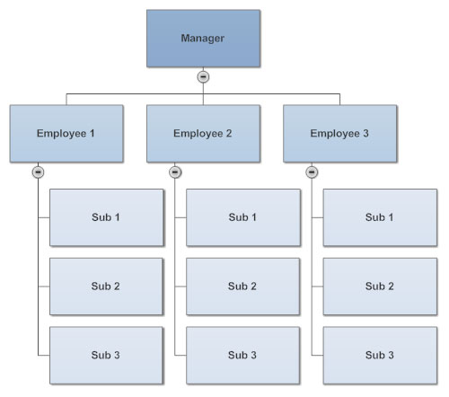
This split of responsibility was very interesting to me; the different levels of people roughly correlated to their experience and level of education (Ph.D. vs. B.S). Therefore, I could see that if I want to be the director, I need to get lots of education (Ph.D.) and lots of experience. For an engineer, it seems that less education / experience is needed.
Summer Projects
At the start of the summer, I was assigned three project areas to chip away at:
- DRM Radio Research
- Wrapping up Monitoring Module from previous summer
- Designing PCB for customer
These projects were all orthogonal to each other in terms of knowledge and scope; they all required different software tools and skills. Having this diversity was nice because it enabled breaks from each project area; I simply switched topics for an afternoon!
DRM Radio Research
To understand the motivation for the DRM radio standard, it helps to understand the current broadcasting landscape across the globe, as well as radio technology in general.
Many different areas of the world use many different radio standards:
- FM, AM, HD Radio: North America
- DAB: Europe, Australia, China, South Africa, many others
- DRM: India
- DMB: Norway, South Korea and Thailand
Silicon Labs offers a portfolio of products that enable designers to tackle this diverse group of radio standards, all within one product family. This shortens time-to-market and makes modular solutions possible.
Aside on Radio Technology
The term “radio” simply defines the usage of electromagnetic (EM) waves to transmit or receive information across space. Radio itself does NOT define the protocols and standards that enable people to use this technology.
Many different protocols and radio standards exist and are in use around the world. These typically change depending on location (government bodies tend to regulate radio frequency (RF) spectrum usage). For example, in the United States, analog AM and FM radio transmissions are very prevalent. Within the last 10 years or so, HD Radio has taken hold of the United States, with nearly all modern cars equipped with HD Radio receivers.
HD Radio
HD Radio is a trademarked term for iBiquity’s in-band on-channel (IBOC) digital radio technology used by AM and FM radio stations to transmit audio and data by using a digital signal embedded “on-frequency” immediately above and below a station’s standard analog signal, providing the means to listen to the same program in either HD (digital radio with less noise) or as a standard broadcast (analog radio with standard sound quality).
There’s a lot in that definition, so let’s unpack it a bit.
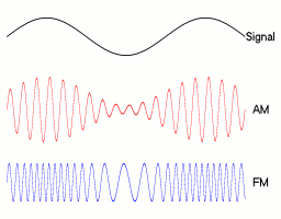
First of all, it’s important to notice the difference between analog and digital radio. Analog radio, like legacy Amplitude Modulation (AM) or Frequency Modulation (FM), encodes audio information directly onto the EM waves. The simplest case, AM, varies the amplitude of the carrier wave (e.g. 1440kHz), but keeps a constant frequency. This is easiest to demodulate on a receiver and get back the original data. FM, by contrast, varies the frequency of the carrier wave, but keeps the amplitude the same. See the animation below for a graphical example.
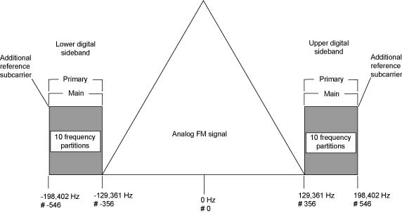
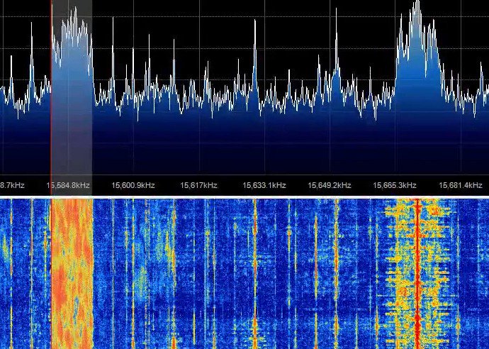
Now back to HD Radio: FM HD Radio defines an extension to simple analog transmission (specifically an IBOC extension), augmenting the signal with digital data. The standard is defined to be backwards compatible, meaning analog-only receivers still work. See the plot below which illustrates the added frequency content for HD Radio digital streams.
Car radios are a common place to receive HD Radio. The radio might initially receive the analog FM stream (because it has the fastest time-to-audio), but then later acquire the digital stream (meaning it locks onto it and starts decoding it). At this point, the receiver can transition the playing analog stream to the digital stream, resulting in improved audio quality.
DRM
Digital Radio Mondiale, or DRM, is a “new” digital radio standard, popular in India. It was developed to replace existing AM broadcasting with a digital alternative. AM broadcasts occupy the medium wave (MW) part of the medium frequency radio band (525 kHz to 1705 kHz); since the wavelengths are so long, buildings and hills do not block signal propagation, nor does the Earth’s curvature. Because of this, broadcasts can be received over large distances.
DRM is designed to be very configurable so that broadcasters can tailor their transmission to adapt to constraints within their target reception area. For example, physical channel impairments like Doppler effect and multipath interference can vary from region to region. DRM broadcasters can increase data robustness to account for these impairments. Some geographical regions also have very crowded spectral bands. DRM can transmit in as little as 4.5kHz bandwidth, but can also be configured to use larger bandwidth for more data throughput.
For comparison, another digital radio standard popular in Europe among many other areas, Digital Audio Broadcast (DAB), has a spectral occupancy of about 1.5 MHz, over 300x the spectral occupancy of DRM! While this isn’t necessarily a fair comparison to DRM (DAB supports many more streams per slot than DRM), it does show that DRM has a very small spectral footprint!
Another intern was also working on DRM; he gave an overview presentation about DRM early in the summer which was very helpful. I worked with him a bit: he used my end-to-end PC DRM receiver for verifying his DRM receiver test-suite (see next project area).
End-to-End DRM Signal Path
My internship happened to occur when Silicon Labs was starting work on a new DRM receiver. The team needed a PC-based platform to start developing algorithms and building blocks for the new firmware. Ideally, the PC-based platform would allow transmitting DRM broadcasts, adding channel impairments, demodulating the signal, and decoding it. If such a platform existed, it would enable developers to evaluate algorithm performance on an easy-to-use platform (i.e. not embedded hardware).
I cobbled together different components to build such a system:
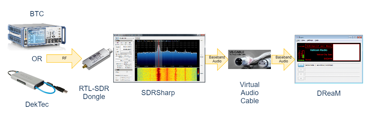
As seen in the diagram above, the signal path starts at a PC, goes out and gets modulated to RF, loops back into the PC, gets demodulated, and finally decoded via the open-source DRM receiver, DReaM.
For development and testing purposes, naturally the team preferred low-cost hardware so that everyone could have a system at their desk. I used the popular RTL-SDR dongle, which is a software defined radio (SDR) USB dongle for open-source SDR development and use.
There was little documentation online about getting this dongle to work with DRM, and the team wanted internal documentation that anyone could follow for getting this set up. I created the documentation and assembled the software tools with little trouble; the scarce online tutorials I could find seemed to work well.
Overall, this was an interesting look into DRM. I learned a lot about this new radio standard and provided a real value add to the team.
DReaM Software Analysis
DReaM software repository website…
After I finished the end-to-end DRM platform, I began studying DReaM, an open-source DRM receiver. This is a C++ application with full Tx -> Channel -> Rx modeling. The team can use this model as a reference implementation, comparing their firmware outputs to “golden” outputs from this model.
Because of the nature of C++, the DReaM software was full of class inheritance and abstractions for encoders/decoders, making it a pain to extract pieces for unit testing. Ideally, blocks of firmware could be unit tested and compared to blocks from the DReaM software.
To aid in rapid development, I looked through the DReaM source code and put together a presentation outlining its design and structure, which I presented to the team.
Monitoring Module
My second project area involved the Monitoring Module, which I started last summer and got a working implementation for team use. Unfortunately, the tracing part was difficult to use, so it sat untouched by the team. This summer, my job was to “productize” the module and give a presentation about using it to teach the team.
There are numerous applications that can run on the Si46xx hardware, so I needed to verify the framework worked correctly on all products in the family. This involved extensive testing as well as updating scripts and the firmware itself.
For example, when operating on “satellite” devices on the Si469x multi-chip module (MCM), all the SPI traffic goes through the master chip, which then forwards the messages to the correct satellite. To run the Monitoring Module on the satellites, I needed to update the scripts to fully support the nature of the communication between chips.
Also, some of the applications do not have the instruction memory available to compile the tracing part of the Monitoring Module. To fix this, I disabled some unused internal RTOS code related to tracing which reduced memory footprint, allowing the binary to fit!
At the end of my testing and improvements, the MM was ready for use. During a team Lunch & Learn, I gave a tutorial presentation about how to use the module.
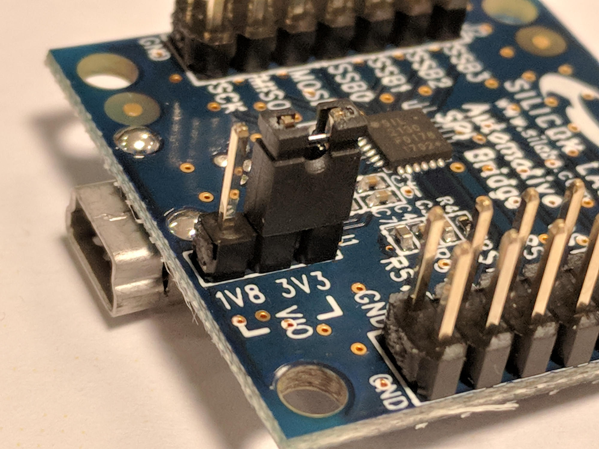
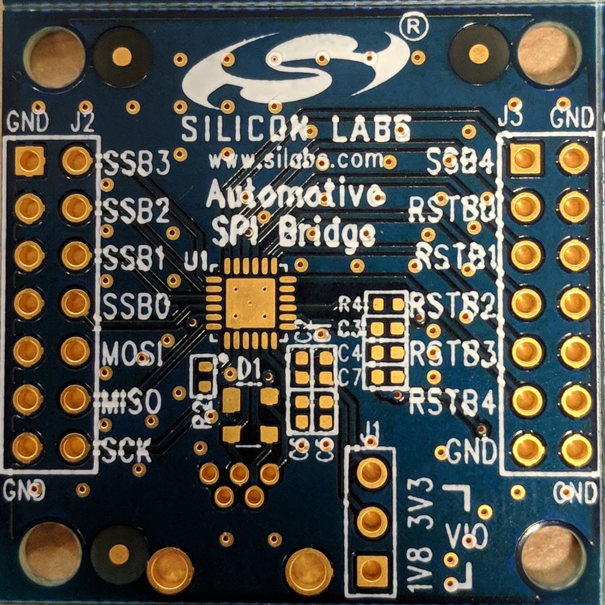
Automotive SPI Bridge PCB
For this project, I was tasked to design a minimally-sized PCB to be used as a SPI bridge between a host PC and SPI devices (namely Silicon Labs’ automotive audio portfolio). I used the Silicon Labs CP2130 device for the brains of the operation. This board design was basically a shrink of the CP2130 evaluation kit; it did much of the same things.
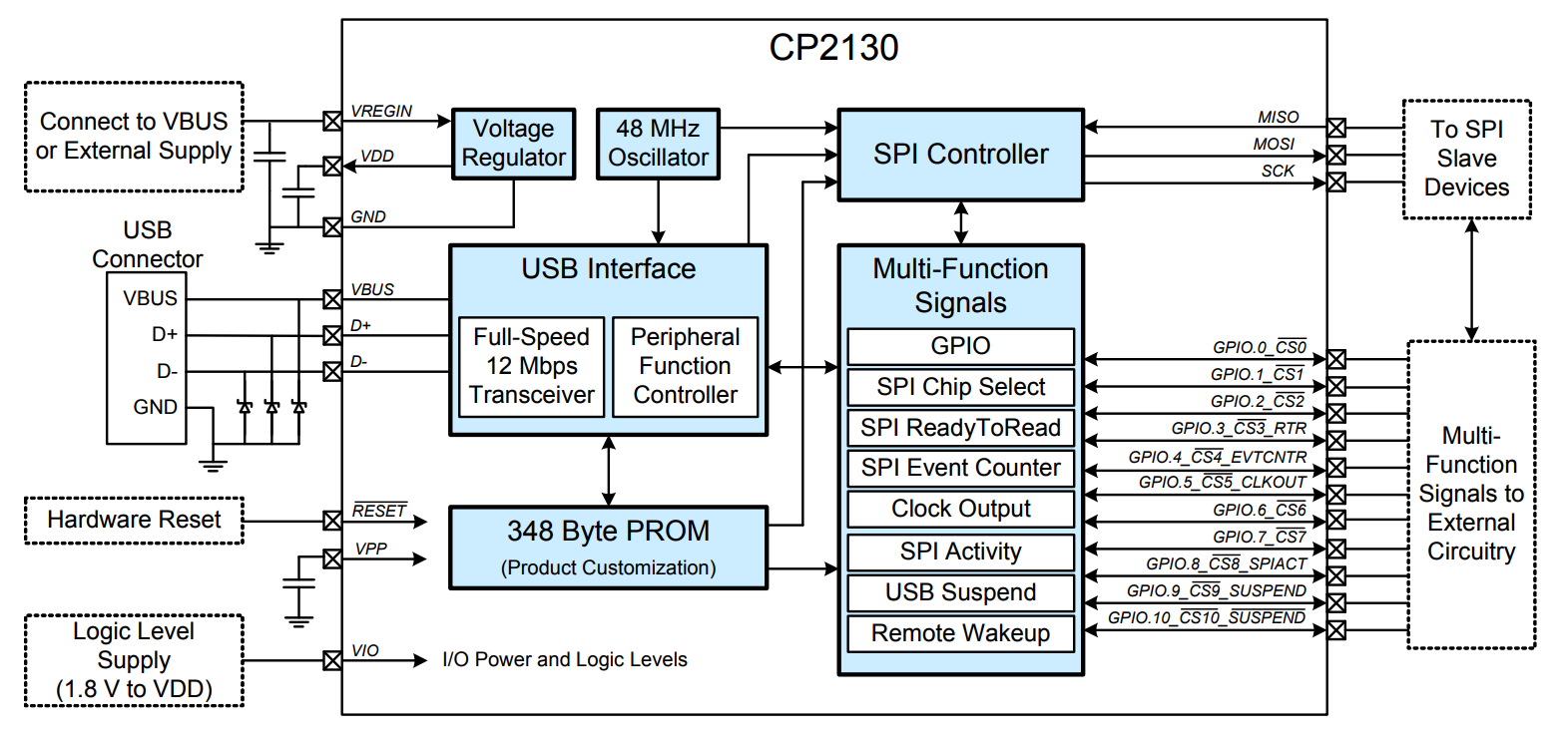
This board was to serve multiple purposes: be mounted on an evaluation board for SPI interface, or mounted in customer car radio head-unit for testing new hardware. Because of this, a few constraints were placed upon its design:
- Small as possible
- Very low RF interference (used to evaluate new radio hardware RF performance; installed right next to device under test)
- Support various I/O voltages
- Very robust physical design (to be used in field)
Throughout the project, I had quite a few design reviews for both the schematic and board layout. These helped me improve the design to arrive at a robust final implementation.
Project Motivation
This project was very different from firmware (i.e. it’s not firmware, it’s hardware). I really wanted to do something like this when I returned this summer for the internship.
Before this, I had designed a few boards on my own, but never to a “standard”; they were all just for personal hobby use. I wanted to see industry standards, have design reviews, see corporate part libraries, use different software tools, etc. During the design process, I made sure to have multiple design reviews and many different opinions to build my knowledge of what to look for in good designs.
Some of my learned skills include:
- Minimizing RF interference
- Optimum component placement for shortest traces
- High speed routing concerns for USB data
- Ground plane stitching on top / bottom
- Designing in silkscreen areas (e.g. company logos)
Overall, I am very pleased with my experience on this project. Even though it was very small and simple, I still learned a lot; the resulting PCB was the most thought-through board I have ever designed.
Thoughts
After returning and interning at Silicon Labs for my second summer, I can safely say that I still love the company. As I said in my previous article, the company values are great, and it feels small enough that each individual employee has a real impact.
Company-Sponsored Learning
As a company, Silicon Labs really seems to care about their employees getting smarter. They periodically hold technical talks and presentations that anyone can sign up for and attend. I view this as an awesome perk of working there.
As a college student and future new employee in the workforce, having a system that enables continued learning is very important to me. Silicon Labs provides that by helping their employees grow along with their careers.
Lunch and Learns
Each team has periodic “Lunch and Learns” where one member of the team presents a topic to the rest of the team. These are a great way to soak up material, plus get free lunch!
I did a presentation on my Monitoring Module towards the beginning of the summer, where I taught everyone what my system was and how to use it. They seemed to find the presentation helpful.
Technical Symposium
Silicon Labs holds an annual internal technical symposium for full-time employees to share their work with other colleagues. This is basically like a research conference, but internal to the company.
All these presentations and talks are recorded and put online for future reference. I found this treasure chest of knowledge and spent some of my spare time soaking up information.
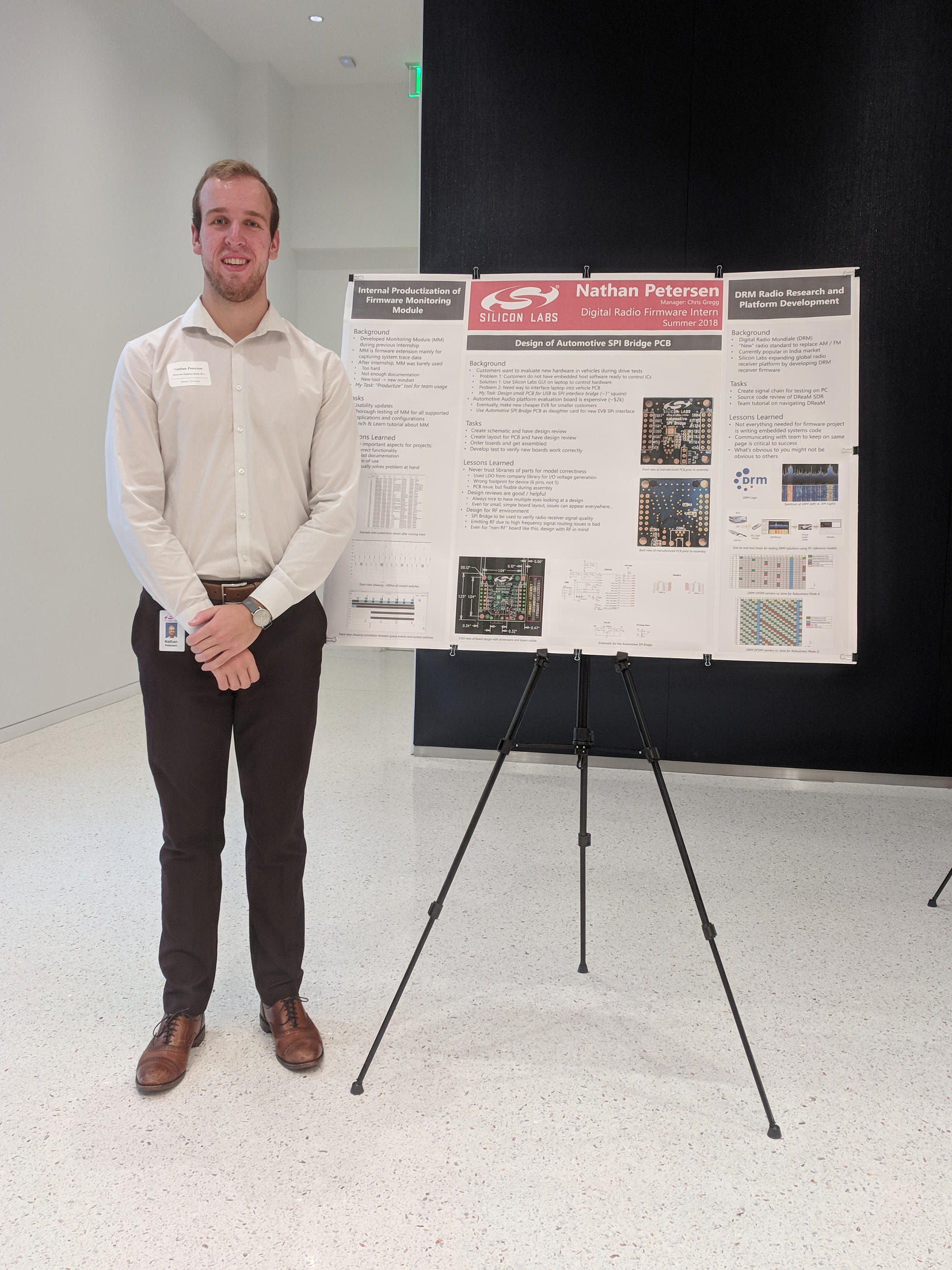
Intern Symposium
Like the main Technical Symposium, the company holds an “Intern Symposium” at the end of the summer for interns to partake in the company-wide knowledge sharing. This is very similar to the “real” technical symposium; interns make posters and present about their summer projects.
Online Recorded Trainings
Along with the Technical Symposium recorded talks, other videos are available online from various trainings and meetings. These include topics related to finance, tech, leadership, etc. I really enjoyed the finance and business talks because of the insights provided about Silicon Labs as a whole.
Daily Grind
Silicon Labs’ “daily grind” seems normal; there are regular meetings to keep people on target, as well as ample time to get individual work done.
Meetings
Each morning, a team “stand-up” was held to discuss daily tasks. At first, these seemed annoying because they interrupted work time, but I soon realized that they helped keep people on track. Everyone went around and shared what they were doing as well as any blockers hindering them.
Each week, a firmware / apps update meeting was held. This was to make sure that the firmware team was doing the things that were important for customers (i.e. fixing show-stopper bugs).
Biweekly was a “sprint” planning meeting. This was to allocate tasks to team members for the next two weeks.
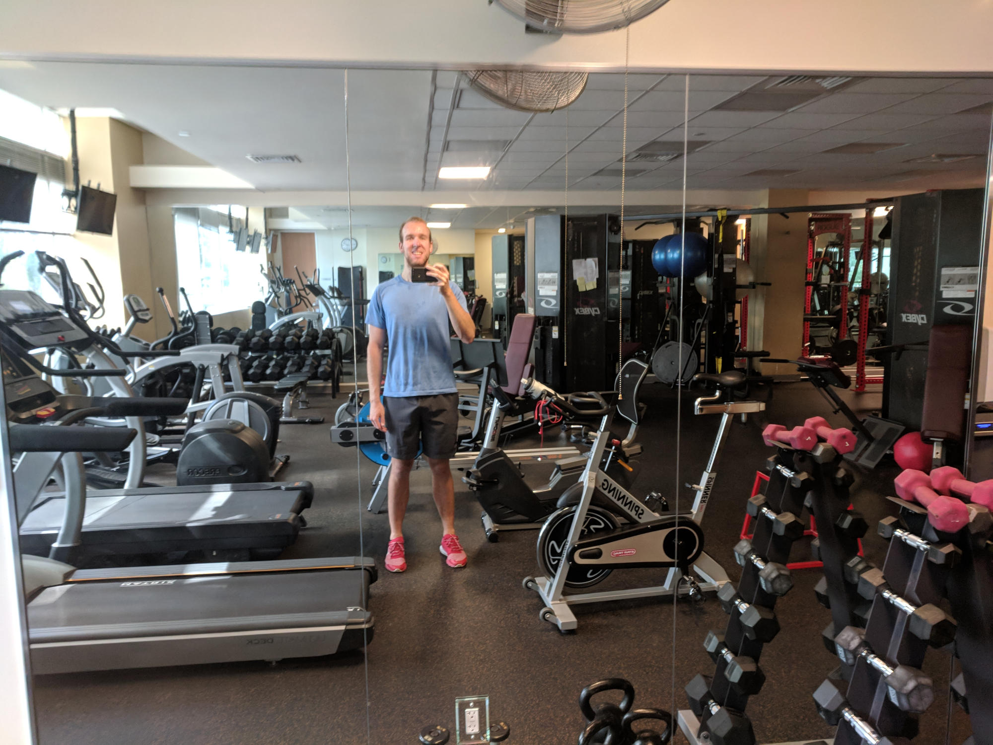
Gym
Silicon Labs has an employee gym located in the office building which anyone can sign up and use at any time. I needed to stay in shape over the summer, so I used it many times…
Customer Interactions
Throughout the summer, there were many times when development was put on hold to service an urgent customer request. With customers trying to go into production using Silicon Labs’ devices, these issues were of the highest priority.
Big customers bring big revenue, which need specialized support for their individual use cases. Interestingly, for large enough customers, the firmware team actually adds new features just for specific requests! What a pain to maintain…
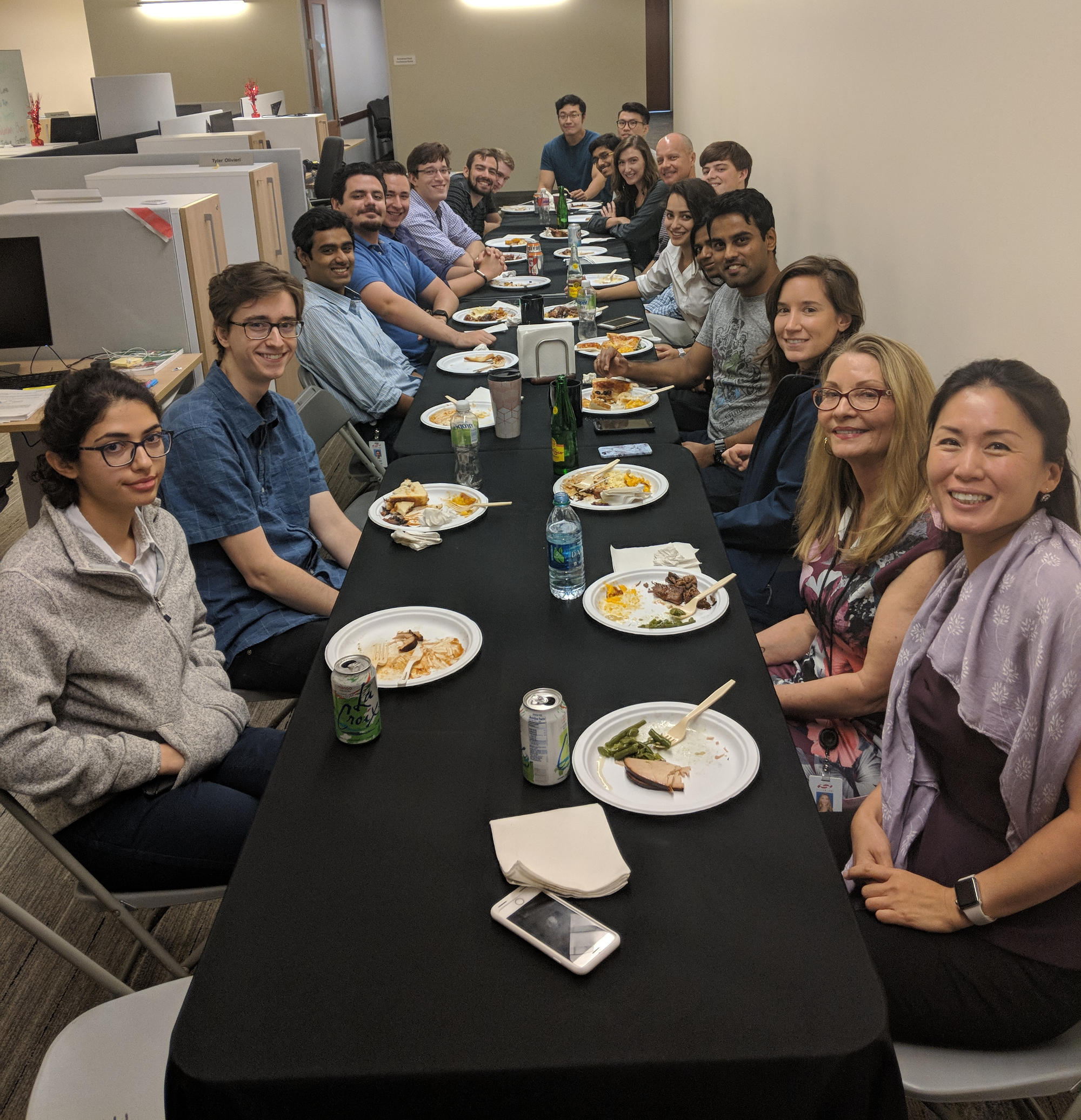
Fun Summer Activities
Not everything this summer was work! I got the chance to explore Austin, and ate at many great places like Terry Blacks and Chuy’s.
One of the lesser known things about Austin relates to the bats that live there. Millions of bats live under the Congress Ave bridge downtown and each night at sunset, they come out and go hunting for food. Because there are so many, the whole ordeal has become quite an attraction for people to come and see:


Future

So, after two summers at Silicon Labs, do I want to work there? Am I going to return?
Yes, I would love to work for the company! They are one of the most respected semiconductor companies in their class and from working for them, I can see why.
Grad School
These past two internships have happened during the summers after my sophomore and junior years of undergrad. I’m planning on applying for grad school, so I probably can’t start a job very soon. Hopefully later, Silicon Labs could still be a good option!
With the provoking of a professor at UW-Madison, I am starting to get interested in power electronics, with emphasis on motor control. If I continue with that, Silicon Labs might not be the best option for employment.
Alternatively, I am broadly interested in embedded systems, with emphasis on the Internet of Things (IoT). IoT seems like a train that’s not stopping, so it makes sense to become an expert in one aspect of it. Silicon Labs has a large IoT division, so if I pursue this option, employment could work.
Summary
Overall, yes, this was a great summer. I enjoyed the work, enjoyed the environment, enjoyed the location, enjoyed the coworkers, enjoyed the other interns, etc, etc, etc.
I’m excited to see what the future holds!
New Post Notifications
If you read this far into this article, you might be interested in subscribing for email notifications about future new posts I write. I will never spam you! Every few months, I write a new article for this website, and will send you email about it. You can unsubscribe at any time. Thank you.