

Designing a Firmware Driver for Serially-Addressable LEDs for Xilinx Zynq-7000
Ever wondered how to control serially-addressable LEDs using the Xilinx Zynq-7000 system-on-chip? Well, this tutorial is for you!
This tutorial discusses the various embedded system layers which exist within the Xilinx Zynq-7000 SoC. It then uses these layers to craft a high-performance RGB LED driver which performs all necessary processing in the FPGA, leaving the DSP resources free for other computations. All source code is publicly available (links are given throughout the tutorial).
Introduction
Over the past few years, I have been developing an open-source control platform (both hardware and firmware) for research motor drives at the University of Wisconsin – Madison. I have written about the hardware a few times on this blog, but never the firmware. That is, until now.
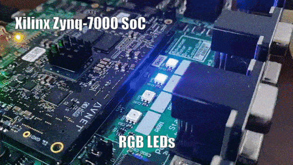
The control platform’s latest hardware design includes a set of four RGB LEDs. The purpose of these LEDs is to give the user the ability to easily show status information from their motor control algorithms in real-time (e.g. solid green means working, flashing red means warning, etc). During the hardware design, the specific LED type needed to be identified; serially-addressable LEDs were chosen due to the benefits described in the next section.
Serially-Addressable LEDs
Serially-addressable LEDs, sometimes referred to as individually-addressable LEDs, are smart. This means that they are not simple discrete parts which illuminate when voltage is applied to them, like normal LEDs. Serially-addressable LEDs consist of both a processor and the discrete LED technology (typically contain three LEDs: red, green, and blue (RGB)). To control the color, the user must toggle the input data pin in such a way that encodes the desired RGB output. The internal processor reads this serial stream of bits and adjusts the LED color outputs accordingly.
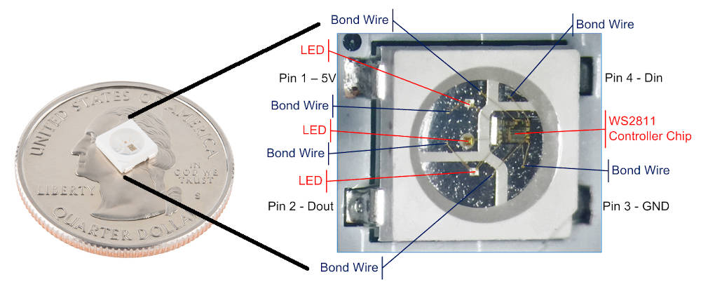
While each device consists of both the processor and discrete RGB LEDs, I will commonly refer to the whole unit as a single LED for simplicity. Adafruit coined the term “NeoPixel” as a general term for serially-addressable LEDs. However, there are many versions of the venerable device: WS2811, WS2812, WS2812B, SK6812, etc. These are commonly sold as strips, but also come as discrete devices; Digi-Key lists 14 different discrete devices! The motor drive controller hardware uses the IN-PI556FCH serially-addressable LED, but they are all pretty much the same (maybe some minor timing differences).
The benefit of these “smart” LEDs is that they can be wired together to form long chains by connecting the data output of one LED to the data input of the next. This minimizes the required processor pins needed and allows single-pin control of an arbitrary number of LEDs. For example, the motor drive controller has four RGB LEDs wired in series.
Xilinx Zynq-7000 SoC
The motor drive controller uses the Xilinx Zynq-7000 system-on-chip (SoC) as the main processor. This SoC is then mounted onto a system-on-module (SoM) which includes the high-speed memory and power supply components. For simplicity, this tutorial will ignore the SoM and assume the LEDs are directly wired to the Zynq-7000 SoC.
What is the Xilinx Zynq-7000 SoC? It is a high-performance device which tightly integrates digital logic fabric (FPGA) with dual-core digital signal processors (DSP). Although it is physically one device, it should be considered two devices: FPGA + DSP. These two devices just happen to be within the same physical package – this is the magic of the system on chip. The DSP runs C code while the FPGA implements custom digital circuitry. As seen in the diagram below, interfacing the DSP with the FPGA requires the use of AXI ports. This interface will be discussed in detail below.

Simplified view of the Zynq-7000 SoC architecture.
System Layers
To build a high-performance firmware driver for serially-addressable LEDs, we need to understand the different embedded system layers that exist in the Zynq-7000 architecture. We will start at the lowest level (closest to hardware) and build up to the highest level (user C code).
Hardware
At the lowest level is the physical hardware. Hardware design is typically done using schematics to conceptually model how physical devices are wired together. A netlist is then created and realized on a printed circuit board (PCB). Once designed, the PCB is fabricated and assembled by soldering the electrical components into place.
When designing at the hardware level, consideration must be made to ensure all devices interact correctly with each other. For a reasonably slow (less than 10 MHz) digital interface consisting of a stream of bits, there is only one major concern: the voltage level must match the requirement from each device. The IN-PI556FCH serially-addressable LED requires 5V digital logic, so the 1.8V output from the Zynq-7000 FPGA pin must be level shifted to 5V. In addition, a power supply decoupling capacitor is used at each LED. The general hardware block diagram is shown below.

Block diagram of hardware required for interfacing FPGA to serially-addressable LEDs. Notice the simplicity – only one FPGA pin is used to control all four LEDs.
FPGA
One step above the physical hardware layer is the field-programmable gate array (FPGA). The FPGA lives in the realm of firmware, but is not explicitly firmware. Conceptually, FPGAs can be thought of as configurable hardware, and are sometimes referred to as “hardware” (e.g. “the processing is done in hardware” can refer to processing done in the FPGA).
The exact abilities of an FPGA change drastically between manufacturers and price points. At low price points, FPGAs typically have simple and limited resources. FPGA resources refer to the various individual digital circuit elements which can be configured to realize the user’s desired logic, such as look-up tables (LUTs) and flip-flops. These are usually combined into standard logic blocks. Expensive FPGAs (like the Zynq-7000 FPGA) tend to include DSP slices which can be used to implement complex math operations in parallel within the FPGA, thus speeding up the application.
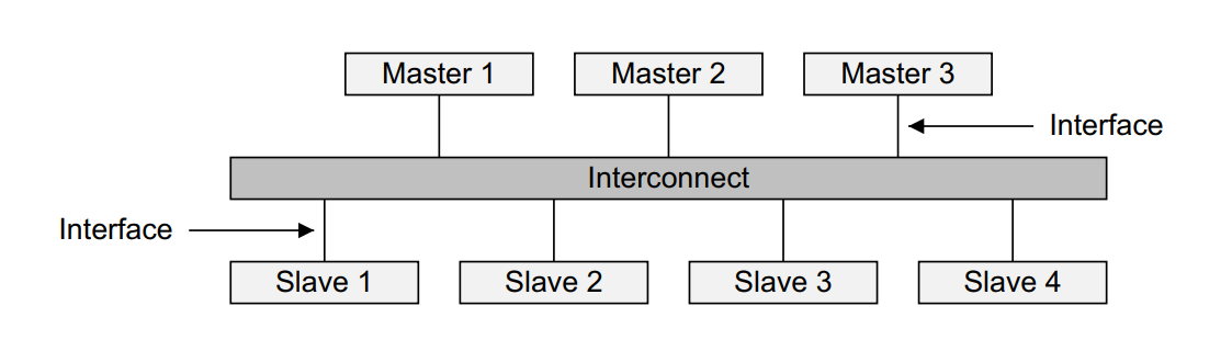
The FPGA resources can be combined into blocks / modules which can implement custom user functionality. These blocks have an external interface (referred to as ports in hardware descriptive languages (HDL), e.g. Verilog). The ports of various FPGA blocks can be wired together to form larger blocks. However, these “raw” HDL block ports cannot easily connect to the DSP. To solve this and enable fast data transfer between the DSP and FPGA, Xilinx implements an industry-standard communication interface called the AXI interconnect.
In order to use this interconnect, FPGA logic blocks must be encapsulated within an IP block. IP, or Intellectual Property, is the term used to describe libraries of digital circuit design used in the FPGA fabric (note that “IP” is an industry term, not a Xilinx term). These libraries are generally low-level interfaces to high-performance hardware (i.e. Ethernet, DDR4 memory, PCIe, etc) which communicate with the main system processor (DSP) via the AXI interconnect.

IP blocks interface with the main DSP using the AXI interconnect.
There exist entire companies who design complex IP blocks which users can buy to enhance their applications. Typically, the hardware descriptive language (HDL) which defines their inner workings is closed-source and proprietary. Xilinx also provides a library of IP that is available from within the Vivado integrated design environment (IDE).
Users can also design and create their own IP blocks. These blocks can implement any custom logic which the user defines. In the Zynq-7000, all IP blocks can communicate with the main DSP using the AXI interconnect. This allows C code to interact with digital logic using various interfaces, such as simple registers or complex data streaming through memory.
The serially-addressable LED firmware driver implements one IP block which allows the main DSP application to control the digital logic within the FPGA by writing to registers. The FPGA then updates the physical LED devices by toggle an I/O pin.
AXI Interconnect
The AXI interconnect is the bus that goes between IP cores and the main processor. AXI is part of ARM AMBA, a family of microcontroller buses first introduced in 1996. AMBA 4.0, released in 2010, includes the second version of AXI, AXI4. Xilinx has adopted the Advanced eXtensible Interface (AXI) protocol for Intellectual Property (IP) cores.
There are three types of AXI4 interfaces:
- AXI4 — for high-performance memory-mapped requirements
- AXI4-Lite — for simple, low-throughput memory-mapped communication (e.g., to and from control and status registers)
- AXI4-Stream — for high-speed streaming data.
The serially-addressable LED firmware driver uses AXI4-Lite since it implements a simple register interface for low-throughput RGB color data.
DSP
The highest layer in the embedded system is the user C code which runs on the digital signal processor (DSP). The C code typically implements the bulk functionality of the user application. For simple applications, bare-metal programming is used (i.e. no operating system (OS)), while complex applications typically use some sort of OS (sometimes a real-time OS, or RTOS).
Within the application C code itself, many layers of abstraction exist. The lowest layer of C code encapsulates the hardware device drivers. These software drivers interface to low-level peripherals, such as status LEDs, analog inputs, or PWM outputs. They define a sensible application programming interface (API) which developers use.
In the Xilinx Zynq-7000 architecture, the C code drivers typically abstract away the raw interface to the FPGA IP blocks. For simple AXI4-Lite based IP, the interface is just memory-mapped writes. These writes go across the AXI interconnect and are read by the IP blocks in the FPGA. This can be thought of as simple register updates.
The serially-addressable LED firmware driver provides a simple C code API which developers can use to control the color and brightness of the RGB LEDs.
Problem Statement
Now that we understand the overall embedded system architecture and the many layers which we have to work with, let’s start to define the problem we are trying to solve.
Goal
The following list summarizes the design goals of this firmware driver:
- Interface with four (4) serially-addressable RGB LEDs.
- Hide the driver implementation from the user (i.e. should be able to swap physical LEDs and update internal driver code without the user knowing).
- Push the LED update routine into the FPGA to save DSP resources.
- Define a simple C code API which is fast and easy-to-use.
These somewhat abstract goals will result in the following C function which the user can call to update the LED colors. Note the simplicity of this interface – this completely hides how the LED is updated.
// User code
// ...
// Set LED0 to be solid red
led_set_color(0, RED);
// ...
Design
The design of the firmware driver will follow the diagram shown below. We only have to create the red and green blocks (C code driver and FPGA IP block). The user C code and physical hardware are out of the scope of this discussion.

Full driver block diagram showing flow from user C code to hardware.
Steps Per LED Update
The following procedure outlines what happens each time the user C code wants to update the color of one of the RGB LEDs.
- User C code calls our C driver for desired LED update…
- Driver sets contents of memory-mapped address…
- Writing to this address kicks off AXI transaction (DSP to FPGA comms)…
- Our FPGA IP block reads AXI bus write data…
- Data processed by our digital circuitry in FPGA…
- Starts our state machine to update LEDs…
- State machine toggles FPGA pin correctly to communicate with LEDs…
- LEDs process stream of bits and update their color output accordingly
Based on these steps, the following sections will go through and design each part of the driver to meet the desired requirements and correct functionality.
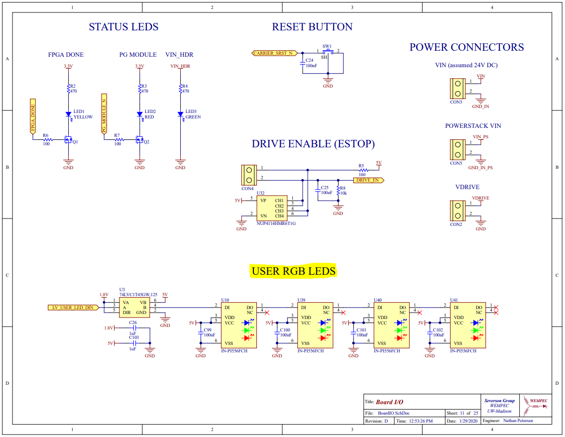
Hardware Design
Since this is a tutorial on firmware design, the hardware design is out of scope. However, for completeness, an example of the hardware schematics is shown below. This simply involves connecting the serially-addressable LEDs in series to a pin on the Xilinx Zynq-7000 SoC.
FPGA Design
The design requirements for the firmware driver dictate that most of the processing time should be pushed into the FPGA to leave the main DSP free to do other computations. This means that the bulk of the design work will happen inside the FPGA using HDL (in this tutorial, Verilog is used).
The goal for this section of firmware design is to craft a complete IP block which can be integrated into the rest of the FPGA design. The IP block implementation requires two parts: 1) AXI interconnect design and 2) custom Verilog LED driver module design. These two parts are discussed below.
AXI Interface Design
The AXI interface for the IP block implements a fairly complex synchronous data transfer protocol. This means that a clock signal is used to align the data transfers between the user IP block and the main AXI bus master. The specification for this protocol is publicly available, however it is a monster to understand (the AMBA AXI spec is 273 pages long).
To help the reader grasp the AXI protocol, a comparison is made to the standard SPI protocol. In the simple SPI protocol, there is a clock line (SCLK), data line (MOSI and/or MISO), and handshaking line (CS). The AXI protocol implements these same basic ideas. However, the advantage of the AXI interconnect is that the width of the data line is much larger, which allows full 32-bit words to be transferred in one clock cycle – there are 32 physical wires between each IP block that connect to the AXI bus. Another major difference between SPI and AXI is that AXI includes address lines. This allows multiple IP blocks to share the same physical bus since the master can transmit a specific address to communicate with each IP block individually.
Each IP block must implement the required HDL for implying the digital logic of the AXI transceiver. Since this digital logic is mainly the same between all IP blocks, the Xilinx Vivado IDE includes a graphical wizard which aids the user in building a generic IP block (access this from Tools > Create and Package New IP...).
Creating IP with Vivado
Depending on the application, a different variant of the AXI protocol can be used: AXI4-Lite, AXI4-Full, or AXI4-Stream. This tutorial will focus on AXI4-Lite which implements a simple register-based data transfer scheme. In the C code, the user writes / reads from a specific memory address which maps to the IP block. In the HDL, the writes update slave registers within the IP block which can then be accessed for the custom digital logic functionality. The C code can also read from the memory address which sends the IP block slave register values back to the DSP.
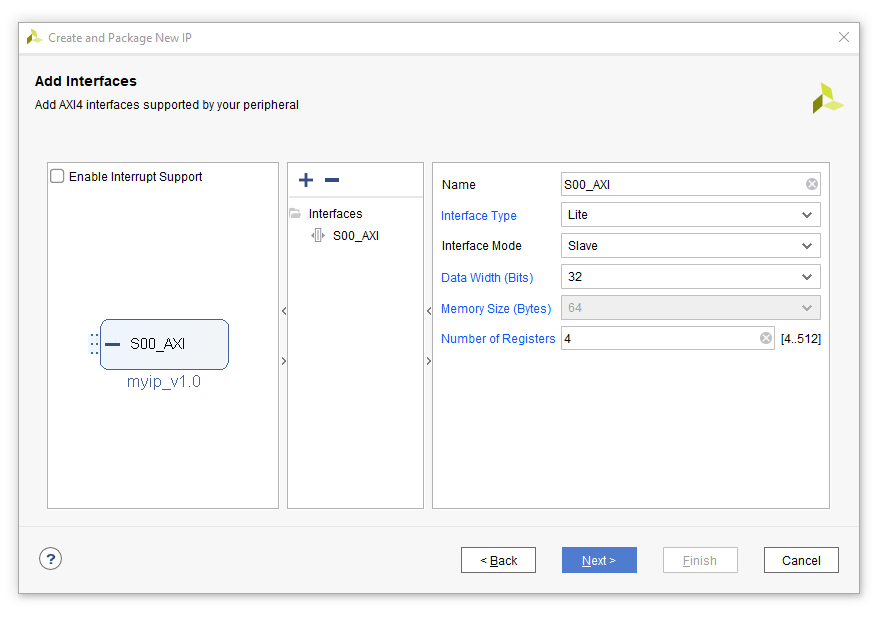
Upon generating the IP block, the user must add it to the block diagram in Vivado. The IDE will then offer to automatically connect the new IP block to the AXI bus and DSP. Once this is complete, the IP block is ready for customization.
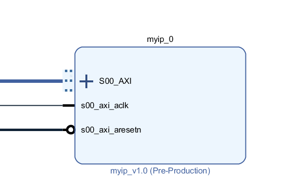
The following image shows the new IP block in the block diagram. Notice that the left side of the block contains the interface for the AXI bus – the visible black signals are the common AXI clock and reset lines. The thick blue signal, S00_AXI, holds all the data, address, and handshaking lines which compose the physical AXI bus. Finally, notice that there are no other I/Os from this block. At this point, the new IP block is simply a collection of four 32-bit registers that are accessible from the DSP. The next section will address how to customize the IP block with the required LED driver functionality.
Custom LED Driver Design
Now that an “empty” IP block is created, the user needs to update it to implement the FPGA application-specific functionality. For this tutorial, each IP block slave register will hold the color state for one RGB LED. Since there are four slave registers and four physical LEDs, this works perfectly.
According to the LED datasheet, each LED requires 24 bits of data which encode the desired color output. Since the LEDs are wired in series, once the first LED receives its color data, it latches it in and then forwards all future data down the line to the next LED.
Since the LEDs communicate using a single data wire (no clock line), specific physical bit patterns are used to encode a logical color data bit (1 or 0). The physical patterns use varying bit widths so that the LEDs can determine the data bit value. All serially-addressable LEDs work like this, but the exact timing varies between manufacturers. The following datasheet excerpt explains how to send a single bit of data to the LEDs.
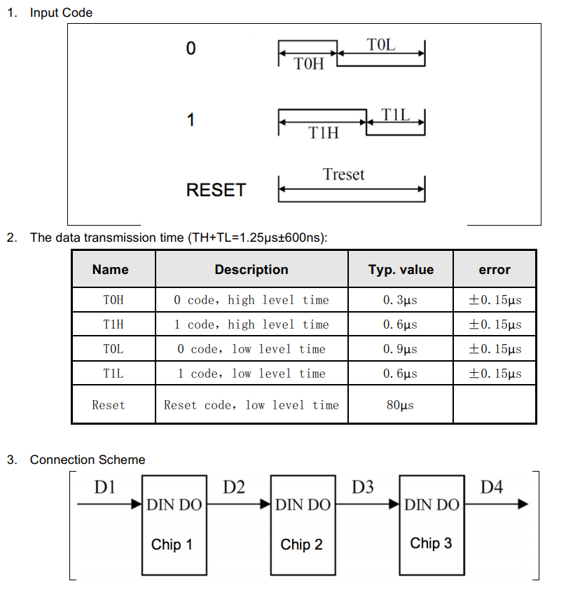
The above diagram shows how to send a single bit to the LEDs. However, the color data is 24 bits long. To send all the color data bits, the FPGA driver should iterate over each bit from the slave registers and create the correct bit pattern, following the above diagrams. The order of the color data bits is presented in the datasheet, with the relevant excerpt shown below.
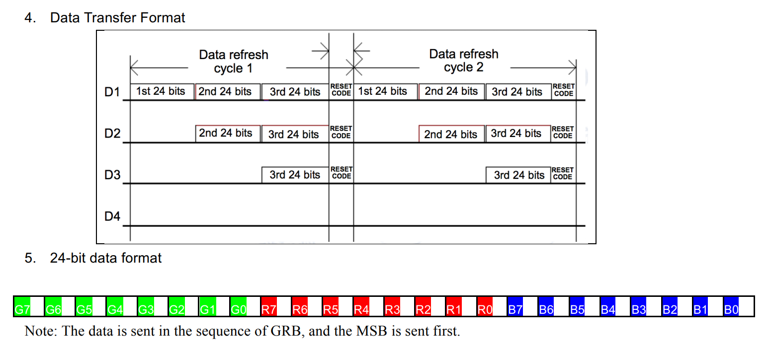
Data is transmitted MSB first and in the following order: green then red then blue. After all the color data bits are sent for a single LED, the RESET pattern is sent which causes the LED to latch in the bits. From then on, the LED will forward new data bits to the next LED in the sequence.
Verilog Modules
For this example tutorial, two Verilog modules are created to drive the LEDs: drv_INPI556FCH.v and line_driver.v. The line_driver block is the low-level module responsible for creating the specific bit patterns as defined in the datasheet. The drv_INPI556FCH block iterates over all the IP slave register color data bits and uses the line_driver to send them across the line.
Source code for these modules is freely available:
AXI / Custom HDL Integration
Once both the AXI bus interface is written (or generated) and the custom HDL modules are finished, they must be integrated together. This logic is usually written at the bottom of the auto-generated AXI implementation file (/hdl/my_ip_block_v1_0_S00_AXI.v). To drive the four RGB LEDs, a state machine is used to iterate across all four IP slave registers. For each register, the color data is transmitted to the LEDs using the drv_INPI556FCH module. The RESET bit pattern is sent between each LED’s color data.
The firmware driver is designed such that the C code does not have to manually trigger the update event to the LEDs. The driver is “smart” – when the IP slave registers are updated, this triggers the transmission automatically. The AXI signal slv_reg_wren is used to detect the update event.
The full integration code can be read here. Note that the first half of the file contains the AXI transceiver implementation and the second half integrates the AXI slave registers with the custom HDL blocks.
DSP Design
Since the firmware driver was crafted where the majority of the LED update computation occurs in the FPGA, the required actions in the DSP are very minimal. The DSP must simply write the proper LED color data to the IP slave registers. When new color data arrives in the slave registers, the IP block automatically streams this data out to the LEDs.
Since the IP block is based around the AXI4-Lite system, writing to the IP slave registers from the DSP is as easy as writing to a memory address. The IP block is referred to as a memory-mapped peripheral.
Each IP block in Vivado is assigned a base address. This address is used to write to the IP slave registers. For example, the RGB LED driver IP base address is 0x43C30000. Xilinx provides utility functions that safely read and write from the memory-mapped peripherals:
// Write to IP slave register
void Xil_Out32(uintptr_t Addr, uint32_t Value);

// Read from IP slave register
uint32_t Xil_In32(uintptr_t Addr);
For this application, we only need to write to the registers, not read. To write to the registers, an offset is added to the base address. An offset of zero corresponds to the first slave register. Note that the offset is in bytes and since each register is 4 bytes long (32 bits), the second register is located at BASE_ADDR + 4.
void led_set(int idx, uint32_t color) {
    Xil_Out32(BASE_ADDR + (idx * 4), color);
}
The example C code driver for the RGB LEDs provides some higher-level functionality to the user. It abstracts away the specific bit ordering for the IP slave registers and allows the user to set the colors based on a color_t typedef.
Source code for the C code driver interface is freely available:
Results
Now that all the driver firmware is written, it needs to be exercised to show that it actually works. The driver code lives in the background as compared to the user C code. The user C code uses the API provided by the drv/led.h file to control the RGB LEDs.
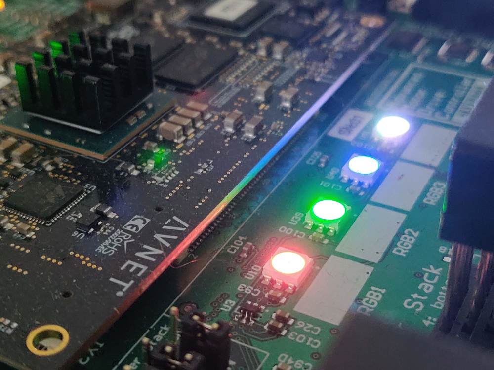
Static RGB Colors
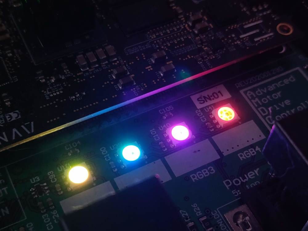
The driver can be used to set static colors to each LED individually, as seen below. This is accomplished using the following pseudo-code:
led_set_color(0, RED);
led_set_color(1, GREEN);
led_set_color(2, BLUE);
led_set_color(3, WHITE);
Real-Time Animation
The user can also create animations using the driver. The following pseudo-code implements an example animation where each LED is illuminated one-by-one in a color chasing manner. Various colors are used throughout the animation.
color_t colors[4] = {RED, GREEN, BLUE, WHITE};
int i = 0;

// Callback function which updates LEDs
// (called at 5 Hz)
void example_callback(void)
{
   led_set_color(0, colors[(i + 0) % 4]);
   led_set_color(1, colors[(i + 1) % 4]);
   led_set_color(2, colors[(i + 2) % 4]);
   led_set_color(3, colors[(i + 3) % 4]);

   if (++i >= 4) {
       i = 0;
   }
}
Summary
This tutorial described the different layers of embedded systems, specifically related to the Xilinx Zynq-7000 SoC architecture. These layers were then used to craft a high-performance firmware driver to control serially-addressable RGB LEDs on an example hardware platform. By understanding the layers of the embedded system, the firmware driver managed to push the LED update overhead into the FPGA, thus not blocking the DSP from running code.
Working Firmware Links
The code in this tutorial is fairly piecemeal, i.e. the reader cannot directly compile and run it. However, the complete working hardware and firmware design for this example driver is open-source and available on GitHub. The hardware schematics are available here (see page 11 for RGB LEDs). The IP block design can be found here with the custom FPGA HDL blocks located here. The C driver code for this IP block is located here.
New Post Notifications
If you read this far, you might be interested in subscribing for email notifications about future new posts I write. I will never spam you! Every few months, I write a new article for this website, and will send you email about it. You can unsubscribe at any time. Thank you.